This thread has been locked.

If you have a related question, please click the "Ask a related question" button in the top right corner. The newly created question will be automatically linked to this question.

AM6548: Accessing DRU configuration registers via PCIe

Part Number: AM6548

Dear TI team,

we're having trouble to understand why we can't write DRU registers (specifically DRU_CHRT_SWTRIG_j) via the PCIe in endpoint mode.

Our setup consists of a x86 CPU in RC mode and an AM6548 in EP mode, with our code running on the R5f.

We sucessfully configured the DRU to perform memory-to-memory copies, and we would like to trigger the actual transfer from the RC (i.e. the x86).

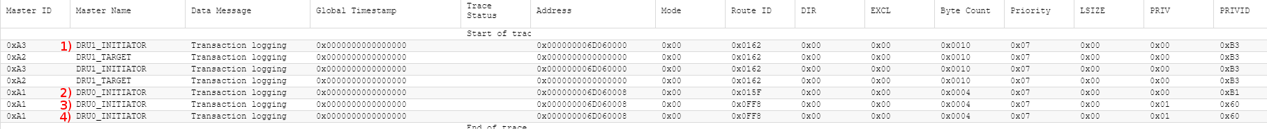
For this we mapped the DRU configuration registers at 0x6D060000 via a PCIe memory BAR. We confirmed that we're able to "see" the DRU config registers, for example by reading the DRU_CHRT_CTL_j registers. However we're unable to write to any of these registers.

When using a different DMA controllers, e.g. NAVSS UDMA, we can write to the respective SWTRIG register (e.g. UDMA_TRT_SWTRIG_j) without problems, and our write triggers the DMA transfer. However for performance reasons we would like to use the DRU, since performance seems to be way better when using the DRU.

We had a look  at the various system interconnect master-slave tables (chapter 3.3.1 Master-Slave Connections in the Rev. E TRM), but we're not sure where to find the DRU in these tables. Since reading from the DRU config registers works we don't think it's a general lack of connectivity.

Since "read only" sounds a bit like a security issue we also looked into the interconnect firewalls, but again we have no idea which firewall would be responsible for writes from PCIe to the DRU config registers.

  • How can we trigger a DRU DMA transfer from an external PCIe RC?
  • Is there a more comprehensive documentation for the firewalls available? We found that the tables lack several firewall IDs for which the TISCI_MSG_GET_FWL_REGION returns configuration information. There are some additional firewall IDs listed in pdk_am65xx_1_0_6\packages\ti\csl\soc\am65xx\dmsc\csl_soc_firewalls.h, but there are also discrepancies between that header and the firewall IDs that we found by querying the SCI client.
  • Is there any other hardware except the interconnect firewalls that could limit our ability to write to the DRU registers from an external PCIe RC?

Regards,

Dominic

  • Dominic,

    Then DRU can be used through the SoC-level UDMA for transfers, which should provide for the most straightforward setup and usage of DRU for the DMA transport. Please take a look at the UDMA-DRU examples in the RTOS SDK package as a basis for your PCIe work and advise if this gives you sufficient detail on configuring for use by the system.

    http://software-dl.ti.com/processor-sdk-rtos/esd/docs/06_01_00_08/rtos/index_device_drv.html 

    6.26. UDMA

    Best regards,

    Dave

  • Hello Dave,

    we really didn't have any issues setting up the DRU transfers, the only issue that we're facing is that we're unable to trigger the transfer via a write to the SWTRIG register via PCIe. We did follow the UDMA-DRU examples, although we used the udma_dru_direct_tr_test example, and I suspect you suggest us to use the udma_dru_test example?

    I guess these two examples refer to these two options mentioned in the TRM:

    The DRU can receive these commands through the following mechanisms:
    • A direct write to the DRU submission registers
    • TR submission over PSI-L from external UDMA-C

    Are you suggesting we use the UDMA TR submission since the UDMA registers are accessible via PCIe, or are there other reasons for using the UDMA TR submission? Do you know WHY we're unable to write the DRU registers from PCIe?

    Regards,

    Dominic

  • Hello Dave,

    we gave the udma_dru_test example a try, but the "software trigger" in that case is still a write to the DRU SWTRIG register, which is our original problem, since we can't write to that register coming from the PCIe bus.

    Can you comment on our original issue, i.e. that we're able to read the registers via PCIe, but can't write them?

    Regards,

    Dominic

  • Dominic,

    There are two layers of firewall permissions for accessing the DRU MMR. The first is the firewall controlling access to the compute cluster config space, and the second is the channelized firewall controlling access to the DRU MMRs. The former should be left open by the System Firmware by default. The latter is to allow control over allocated channels only.

    Please confirm if you have looked to the DRU MMR FW settings. The addresses for these are listed in the TRM section 10.5.7 DRU_MMR_FW Registers

    Some text from section 3.3 below
    3.3.3 Interconnect Firewalls
    The device protection depends on firewalls. They are used to protect data and configuration spaces by managing the accesses to these memory regions.There are two types of firewalls - region based and channelized. There aren't channelized firewalls on system level. Only NAVSS0, MCU_NAVSS0 and DRU0 have channelized firewalls for the various DMA channels. Only region based firewalls are available on system level. See Section 3.3.3.1 and Section 3.3.3.2 for description of the region based and channelized
    firewalls.

    Almost all slaves have a firewall right before the transaction reaches them. There are few exceptions such as WKUP_DMSC0, NAVSS0 and MCU_NAVSS0 slave ports. These subsystems contain local interconnect with own firewalls inside the subsystem itself. The firewalls inside compute cluster (for CC_ARMSS0, CC_ARMSS1 and DRU) are also an exception. They are put on the master instead on the slave port side. To enable access for that master port to the slaves these master side firewalls must individually be programmed.

    ...

    The channelized firewall is associated with the following registers:
    • *_CH_i_CONTROL, where "i" can be from 0 to 63 and denotes the channel. For example, see Section 10.5.7.7 in Section 10.5 Data Routing Unit (DRU). This register is equivalent to the CBA_CONTROL_i_j register of the region based firewall.
    • *_ CH_i_PERMISSION_x, where "i" can be from 0 to 63 and denotes the channel and "x" can be 0 to 2. For example, see Section 10.5.7.8 in Section 10.5 Data Routing Unit (DRU). This register is equivalent to the CBA_PERMISSION_i_j_x register of the region based firewall.

    Best regards,

    Dave

  • Hello Dave,

    these firewalls seem to be all disabled. Also we're not getting any exceptions logged. We manually configured a different firewall to block access to DDR memory, and got the expected errors logged, so I suppose we're looking at the right registers for FW configuration and logging.

    We're currently trying to figure out if the problem is due to the size of the write transactions. While we're only executing 32-bit wide accesses on the x86 we see 16-byte accesses in a "Transaction logging" trace (last column shown is "Byte Count"):

    This shows a write to offset 0x8 on a PCIe BAR that is set up to map 0x6d060000, followed by a read of the same word:

    I'm not sure if we're chasing ghosts here, e.g. if the transaction logging feature is being fooled. If we're executing these accesses using the debugger or the R5f core though, the transaction size is 4 bytes in length:

    Write using "CS_DAP_0" ...memory.writeWord (I'm assuming this uses the DAP's AHB master):

    Write using activeDS.memory.writeWord (I'm assuming this uses the R5f processor):

    Write using application running on the R5f:

    My guess is that somewhere (within the x86, within the PCIe EP, within some interconnect) my 32-bit access is translated to a larger burst with only certain byte enables set - no idea if that makes any sense at all - and that the DRU registers are unable to handle this kind of transaction, while the UDMA registers are able to cope with that.

    I've checked writes to DDR memory and MCU SRAM, too, and all writes via the PCIe EP reach the target with a Byte Count of 0x10.

    I've also checked that even though the transaction log sees a 16-byte write with a 16-byte aligned address (6D060000 when writing to 6D060008), only the desired bytes get actually written.

    It would be great if you could confirm or refute my assumptions:

    • Is it possible that the PCIe controller or the AXI <-> VBUSM bridge within the PCIE subsystem translates our 32-bit write to a 128-bit write with only certain byte enables set?
    • Is there any documentation of the CBA/VBUSM, e.g. what kind of transactions it supports?
    • Is it possible that this 128-bit write (with byte-enables) poses a problem for the DRU registers, but can be handled just fine by the UDMA controller for example?

    Best Regards,

    Dominic

  • Hello Dave,

    these firewalls seem to be all disabled. Also we're not getting any exceptions logged. We manually configured a different firewall to block access to DDR memory, and got the expected errors logged, so I suppose we're looking at the right registers for FW configuration and logging.

    We're currently trying to figure out if the problem is due to the size of the write transactions. While we're only executing 32-bit wide accesses on the x86 we see 16-byte accesses in a "Transaction logging" trace (last column shown is "Byte Count"):

    This shows a write to offset 0x8 on a PCIe BAR that is set up to map 0x6d060000, followed by a read of the same word:

    I'm not sure if we're chasing ghosts here, e.g. if the transaction logging feature is being fooled. If we're executing these accesses using the debugger or the R5f core though, the transaction size is 4 bytes in length:

    Write using "CS_DAP_0" ...memory.writeWord (I'm assuming this uses the DAP's AHB master):

    Write using activeDS.memory.writeWord (I'm assuming this uses the R5f processor):

    Write using application running on the R5f (same Route ID as before, so probably the same initiator):

    My guess is that somewhere (within the x86, within the PCIe EP, within some interconnect) my 32-bit access is translated to a larger burst with only certain byte enables set - no idea if that makes any sense at all - and that the DRU registers are unable to handle this kind of transaction, while the UDMA registers are able to cope with that.

    I've checked writes to DDR memory and MCU SRAM, too, and all writes via the PCIe EP reach the target with a Byte Count of 0x10.

    I've also checked that even though the transaction log sees a 16-byte write with a 16-byte aligned address (6D060000 when writing to 6D060008), only the desired bytes get actually written.

    It would be great if you could confirm or refute my assumptions:

    • Is it possible that the PCIe controller or the AXI <-> VBUSM bridge within the PCIE subsystem translates our 32-bit write to a 128-bit write with only certain byte enables set?
    • Is there any documentation of the CBA/VBUSM, e.g. what kind of transactions it supports?
    • Is it possible that this 128-bit write (with byte-enables) poses a problem for the DRU registers, but can be handled just fine by the UDMA controller for example?

    Best Regards,

    Dominic

  • Hello Dave,

    these firewalls seem to be all disabled. Also we're not getting any exceptions logged. We manually configured a different firewall to block access to DDR memory, and got the expected errors logged, so I suppose we're looking at the right registers for FW configuration and logging.

    We're currently trying to figure out if the problem is due to the size of the write transactions. While we're only executing 32-bit wide accesses on the x86 we see 16-byte accesses in a "Transaction logging" trace. I'm not sure if we're chasing ghosts here, e.g. if the transaction logging feature is being fooled. If we're executing these accesses using the debugger or the R5f core though, the transaction size is 4 bytes in length:

    1) shows a write to offset 0x8 on a PCIe BAR that is set up to map 0x6d060000, followed by a read of the same word

    2) shows a write using "CS_DAP_0" ...memory.writeWord (I'm assuming this uses the DAP's AHB master)

    3) shows a write using activeDS.memory.writeWord (I'm assuming this uses the R5f processor)

    4) shows a write using application running on the R5f (same Route ID as before, so probably the same initiator)

    My guess is that somewhere (within the x86, within the PCIe EP, within some interconnect) my 32-bit access is translated to a larger burst with only certain byte enables set - no idea if that makes any sense at all - and that the DRU registers are unable to handle this kind of transaction, while the UDMA registers are able to cope with that.

    I've checked writes to DDR memory and MCU SRAM, too, and all writes via the PCIe EP reach the target with a Byte Count of 0x10.

    I've also checked that even though the transaction log sees a 16-byte write with a 16-byte aligned address (6D060000 when writing to 6D060008), only the desired bytes get actually written.

    It would be great if you could confirm or refute my assumptions:

    • Is it possible that the PCIe controller or the AXI <-> VBUSM bridge within the PCIE subsystem translates our 32-bit write to a 128-bit write with only certain byte enables set?
    • Is there any documentation of the CBA/VBUSM, e.g. what kind of transactions it supports?
    • Is it possible that this 128-bit write (with byte-enables) poses a problem for the DRU registers, but can be handled just fine by the UDMA controller for example?

    Best Regards,

    Dominic

  • Dominic,

    Thanks for the very detailed follow up. Just to confirm from your post, you have checked that you are able to properly trigger the DRU from the debugger and from an R5F application? This does reinforce your point on the firewalls being disabled so we can rule that out.

    Let me check now on the PCIe transactions specifically and if we can reproduce the same and give guidance on a quick resolution.

    Best regards,

    Dave

  • Hello Dave,

    yes, we can trigger the DRU by writing to 0x6d06xxx8 (the actual address depends on the channel we got from the UDMA driver) from the R5f application, but not when writing via PCIe.

    Regards,

    Dominic

  • Dominic, 

    Dave assigned me to check on the PCIe master port burst limitations. I am checking on some internal documents. So far it seems all 0x6d06xxx8 addresses you are access satisfies the 8-byte alignment requirement. Could you also confirm if you tried to submit non-atomic TRs by the host via the PCIe BAR0?

    regards

    Jian

  • Hello Jian,

    thanks for looking into this.

    jian35385 said:
    Could you also confirm if you tried to submit non-atomic TRs by the host via the PCIe BAR0?

    Not sure what you're trying to say here. Should we re-run the test with BAR0? We've been using BAR2 before. If you're just asking whether our request might have been an atomic access: No, it's a plain 32-bit pointer write.

    jian35385 said:
    the 8-byte alignment requirement

    What 8-byte alignment requirement are you refering to?

    Do you have any insight whether my access appears with a 16-byte length in the transaction log?

    Regards,

    Dominic

  • Dominic, 

    We had a review with our PCIe Controller Subsystem owner. He confirmed that the PCIe controller will not "pad" or "combine transactions". So the trace file showing transactions to 6D060000 when writing to 6D060008 is not expected, point to some alignment related behavior.

    From you notes, I was not able tell if you ever tried to write to the DRU_CHRT_CTL_0 register, at address 0x6D060000 (Enable, Teardown or Pause bits are R/W), and see if you can issue an 8-byte write to this register. 

    To your earlier question of bus transaction limitations, Section 12.2.2.4.6.2, "PCIe Transaction Limitations" of the TRM (Version E), give some descriptions of the behaviors of the controller bridges and master ports. 

    Also can you share following details of your program:

    1. which BAR did you use to map the DRU registers?

    2. from X86 side, how was the write transaction is programmed? do you program a single 8-byte write, or two 4-byte write?

    thanks

    Jian

  • Hello Jian,

    jian35385 said:
    We had a review with our PCIe Controller Subsystem owner. He confirmed that the PCIe controller will not "pad" or "combine transactions". So the trace file showing transactions to 6D060000 when writing to 6D060008 is not expected, point to some alignment related behavior.

    I've performed some more testing using the DDR memory as my target, mapped via BAR2. I'm using the "devmem2" utility on the linux command line, which I extended to be able to read/write 64-bit values.

    Here's my command line output on Linux:

    root@target:~# devmemX 0x92500000 l 0x4444333322221111
    root@target:~# devmemX 0x92500008 l 0x4444333322221111
    root@target:~# devmemX 0x92500004 w 0x55556666
    root@target:~# devmemX 0x9250000c w 0x77778888
    root@target:~# devmemX 0x92500000 l
    0x5555666622221111
    root@target:~# devmemX 0x92500008 l
    0x7777888822221111

    And this is what the SoC transaction trace sees:

    The memory gets written just fine, even 32-bit writes only write to the intended bytes, but in the transaction log it all shows up as 16-byte long accesses.

    The actual accesses in devmem2 look like this (showing just the pointer dereferencing):

                    *((volatile uint32_t *) virt_addr) = writeval;
                    *((volatile uint64_t *) virt_addr) = writeval;
                    read_result = *((volatile uint32_t *) virt_addr);
                    read_result = *((volatile uint64_t *) virt_addr);
    

    jian35385 said:
    From you notes, I was not able tell if you ever tried to write to the DRU_CHRT_CTL_0 register, at address 0x6D060000 (Enable, Teardown or Pause bits are R/W), and see if you can issue an 8-byte write to this register. 

    I just tried that, and it didn't work either:

    root@target:~# devmemX -r 0x92600000 l 0x80000000
    Written 0x0000000080000000; readback 0x0000000000000000
    root@target:~# devmemX -r 0x92600000 l 0x40000000
    Written 0x0000000040000000; readback 0x0000000000000000
    root@target:~# devmemX -r 0x92600000 l 0x20000000
    Written 0x0000000020000000; readback 0x0000000000000000

    BAR5 maps to 0x6d060000. The channel that I got assigned from the DRU UDMA driver is located at +0x1400, and I can see that this channel is enabled:

    root@target:~# devmemX -r 0x92601400 l
    0x0000000080000000

    I'm also unable to teardown this channel:

    root@target:~# devmemX -r 0x92601400 l 0x40000000
    Written 0x0000000040000000; readback 0x0000000080000000

    jian35385 said:
    To your earlier question of bus transaction limitations, Section 12.2.2.4.6.2, "PCIe Transaction Limitations" of the TRM (Version E), give some descriptions of the behaviors of the controller bridges and master ports. 

    The restrictions outlined there shouldn't be a problem for the kind of access I'm trying to perform.

    I found that the TRM mentions that the PCIe bridges (at least the VBUSM2->AXI bridge, but I'm guessing the same is true for the other direction) is 128 bits wide, which would be exactly the 16 bytes I'm seeing in the transaction log...

    jian35385 said:

    1. which BAR did you use to map the DRU registers?

    2. from X86 side, how was the write transaction is programmed? do you program a single 8-byte write, or two 4-byte write?

    1.) The DRU registers are mapped via BAR5 in this case

    2.) I used 32-bit writes before, but your comments made me realize that the DRU registers are actually 64-bits long, so I changed them to 64-bit writes, unfortunately with the same results.

    Regards,

    Dominic

  • Hello Jian,

    I tried to further debug this, first using the DRU firewall, then using PCIe AER header logging, but unfortunately I haven't come very far.

    After restricting access to the DRU using the firewall, I was able to see my access getting logged, the x86 returned all 0xff, and the PCIe endpoint set the SIGNALED_TARGET_ABORT.

    • Just like the transaction log the firewall shows all accesses aligned to 16 bytes
    • The firewall shows all READ accesses as 16 bytes long, no matter whether I try to read/write 1, 2, 4, 8 or 16 bytes.
    • The firewall shows my WRITE accesses as 8 bytes long, no matter whether I try to read/write 1, 2, 4, 8 or 16 bytes.
    • My access to the DRU_CHRT_* registers at 0x6d06nnnn show up with a target address of 0x0008nnnn. Addresses up to 0x6d05fff0 show up un-shifted, at 0x60000 the addresses seen by the firewall have an offset of 0x20000. No idea if that's relevant. Apart from that, accesses to other parts of the DRU region are seen the same way by the firewall, i.e. aligned to 0x10, size 16 for reads and 8 for writes.

    I have no idea if there's anything in the x86 (RC) that could cause my requests to be delivered to the AM65x that way. I tried to (ab-)use the PCIe advanced error logging to have my TLP logged, but haven't been successful that way. I managed to have my accesses treated as CA (completer abort) or UR (unsupported request), and I get the HEADER_LOG_OVERFLOW_STATUS bit set, but the Header Log registers always contain 0. The devmem utility is using /dev/mem with O_SYNC and should thus treat the memory as "uncacheable".

    Apart from the size of the access I noticed a few more differences in the transaction log:

    • The Privilege is 0 (User) for accesses coming from PCIe, and 1 (Supervisor) for access from the R5f.
    • The Data Type is 2 (DMA) for accesses coming from PCIe, and 0 (CPU) for access from the R5f.
    • The Sharability is 0 (Non shareable) for accesses coming from PCIe, and 3 (System) for accesses from the R5f.
    • The Secure field is 0 (not secure) for accesses coming from PCIe, and 1 (secure) for accesses from the R5f.
    • The Memory Type is 1 (Normal WB cacheable) for accesses coming from PCIe, and 0 (device) for accesses from the R5f.

    The differences could also be a reasonable explanation for the behaviour I'm seeing, but I have no idea how to influence these attributes of my accesses.

    Any help would be appreciated.

    Regards,

    Dominic

  • Dominic, 

    I used to have a pair of EVM cross-connected via a PCIe cable, so if we suspect the RC is packing outbound transactions, we may try a different RC for comparison. But currently my other EVMs are in the shop and not been returned yet. If you happen to have multiple EVMs, I can point you to the cable I used. 

    Also can you clarify how to use "PCIe AER header logging", are you enabling the function in the RC kernel or EP? 

    Thanks

    Jian

  • Hello Jian,

    unfortunately I have only my custom hardware right now. We have multiple EVMs, but I can't work with those at the moment. It would still be nice if you could show me which cable you used, so that maybe I can organize to have that as a fallback. Is it this?

    jian35385 said:
    Also can you clarify how to use "PCIe AER header logging", are you enabling the function in the RC kernel or EP? 

    As far as I understand AER the AM65x implements AER to provide details about errors. I configured an inbound ATU to return CA or UR, and these errors then got set in the AER registers, e.g. "Unsupported Request Error Status" in "Uncorrectable Error Status Register" and the "First Error Pointer" in "Advanced Error Capabilities and Control Register" was set to 0x14. The way I read the specification (never tried this before) the EP should also log the TLP of the transaction causing the error, but I can only see the "Header Log Overflow" bit getting set.

    Regards,

    Dominic

  • Dominic, 

    The cable you pointed above is what I used. The modifications was to remove the REFCLK, as both EVMs would have their own REFCLK. 

    I was occupied during the day and did not get time to read more on AER. One question was bothering me, where you mentioned:

    • The firewall shows all READ accesses as 16 bytes long, no matter whether I try to read/write 1, 2, 4, 8 or 16 bytes.
    • The firewall shows my WRITE accesses as 8 bytes long, no matter whether I try to read/write 1, 2, 4, 8 or 16 bytes.

    Is this also true for RC transactions to a regular memory region, say MSMC SRAM region? If answer is yes, then we can focus on RC packing, if answer is no, then we can focus on EP, thoughts?

    Jian

  • Hello Jian,

    I verified the effect on the firewall logging again, and the behaviour is different between writing to the DRU region and writing to DDR memory.

    READs and WRITES to DRU registers mapped via BAR5 are logged as 16 bytes for READs and 8 bytes for WRITEs.

    READs and WRITES to DDR registers mapped via BAR2 are logged as 16 bytes for READs and WRITEs.

    I'm accessing addresses at an offset +0x8, but the logged address is always 0x10 bytes aligned, for READs and WRITES to both DRU and DDR memory. This could mean that the WRITE transaction to the DRU arrives as 16 bytes at the DRU firewall, but is split into two 8 byte writes at the firewall. Also the transaction trace doesn't show a difference for READs and WRITEs to the DRU registers.

    If I block access to the DRU for the R5f the transaction gets logged with the correct address and size.

    I guess we'll be able to trace the PCIe transactions on the bus, but that wont happen before next week.

    Can you comment on the differences between PCIe and R5f access visible in the transaction log?

    Dominic Rath said:

    Apart from the size of the access I noticed a few more differences in the transaction log:

    • The Privilege is 0 (User) for accesses coming from PCIe, and 1 (Supervisor) for access from the R5f.
    • The Data Type is 2 (DMA) for accesses coming from PCIe, and 0 (CPU) for access from the R5f.
    • The Sharability is 0 (Non shareable) for accesses coming from PCIe, and 3 (System) for accesses from the R5f.
    • The Secure field is 0 (not secure) for accesses coming from PCIe, and 1 (secure) for accesses from the R5f.
    • The Memory Type is 1 (Normal WB cacheable) for accesses coming from PCIe, and 0 (device) for accesses from the R5f.

    Regards,

    Dominic

  • Dominic, 

    I am trying to read more into how the transaction log is interpreted, as all the attributes are associated to CPU transactions. For example, the last bullet in your list, not sure how the PCIe transaction to DRU is logged as a cacheable access. 

    Also I got my other EVMs back and have my two EVMs connected. I need some software changes as one of the EVM is a newer silicon revision. May take several days to get software working.  

    regards

    Jian

  • Hello Jian,

    we've verified the TLPs coming from the x86 using a PCIe analyzer, and the transactions seem to be just fine.

    We tried reading/writing 8, 16, 32 and 64 bits aligned to 0x...0, 0x...4 (not for 64-bit) and 0x...8, and the accesses appear as MRd(32) TLPs with a length of 1 or 2 and the appropriate 1st/last byte enables set. The address is always the actual address read or written (0x...0, 0x...4, 0x...8).

    In the SoC transaction log the accesses appear as 0x10 bytes long with an address aligned to 0x...10).

    Could you verify again with your colleagues if there's anything in the PCIe EP implementation, maybe the AXI2VBUSM bridge that could explain this behavior?

    It would also be interesting to know why this poses a problem for the DRU but not for the MAIN or MCU UDMA registers (if the transaction length really is the issue).

    Regards,

    Dominic

  • Dominic, 

    Just a quick update that i have not received the responses on PCIe transactions vs. R5. Will let you as soon as I get them. 

    Jian

  • Hello Jian,

    has there been any progress on this issue?

    Regards,

    Dominic

  • Dominic, 

    Just an update - I've not received the replies yet on the master port transaction. In parallel, I tried to get my board-to-board setup, it was bare metal code that was built with older version of the CSL, I ran into an issue with the lib compatibility and resolving it. 

    Will update on both front later this week. 

    JIan 

  • Dominic, 

    Finally I got my boards setup and connected. But I immediately run into firewall constraints though I am using a GP device.  Also my colleague still believes "The firewall you need to program is the firewall in front of the North bridge for MSMC region". So I will check locations of these firewall regions on my setup in the next day or so. 

    Jian

  • Donimic, 

    I did not get a chance to debug my board. If you are ahead of me, can you check your firewall configuration of:

    Slaves Config Idx IOFW Regions IOFW Priv IDs IOFW ID Has Firewall or notf
    navss256l.main_0.nav_nb0_bp 760 24 3 2808 Y

    Chunhua was suspecting this firewall causing the problem - it is controlling the path from PCIe HP port to NorthBridge0. Also can you confirm if you are using PCIe HP port or the default LP port?

    thanks

    jian

  • Dominic, 

    Field team indicated this issues has not been resolved. I have my EVM-EVM setup alive again and ready to debug. 

    Let me know if you have any update on your end over the long dormant time. 

    regards

    Jian

  • Hello Jian,

    the issues is still open. If we were able to directly write to the DRU registers from the x86 RC we would be able to improve performance a lot for our use case.

    We haven't made any progress here, but I wouldn't know what to look for anyway.

    We've confirmed that the transaction is perfectly fine on the PCIe bus using a PCIe analyzer, and that is has unexpected properties when logged by the firewall or by the transaction log.

    Please note that the firewalls only logged something when I specifically disallowed access from the PCIe port, i.e. this was just a means to debug the issue by looking at how the transaction is seen at the firewall.

    My last theory was that the transaction that is put on the AM6x internal busses by the AXI2VBUSM is in some way incompatible to how the DRU expects to be accessed. Since the internal bus system is barely documented there wasn't much I could try anymore.

    I wont be in the office until January 7th.

    Regards,

    Dominic

  • Dominic, 

    I will do some experiment on my board and update. 

    Jian

  • Dominic, 

    To confirm which path was used to get to the DRU register, do you recall your BAR registers settings? If you can send how the BARs were configured by the RC, I can try to figure out HP/LP. sorry it has been a while i need to refresh. 

    Jian