This thread has been locked.

If you have a related question, please click the "Ask a related question" button in the top right corner. The newly created question will be automatically linked to this question.

DAC38RF97: dac no output

Part Number: DAC38RF97
Other Parts Discussed in Thread: LMK04828

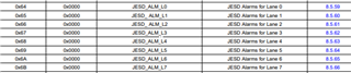
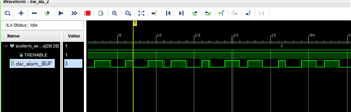
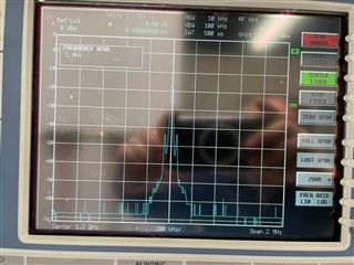
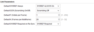
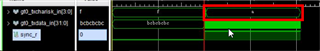
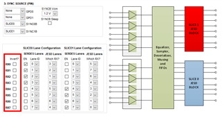
We are using this DAC38RF97 part in our radio project.  Our design mainly based on the TI's reference design.  We are having problem of NO OUTPUT.  We have checked all voltages and they are normal and correct based on the data sheet.  The SerDes inputs to the DAC is from Xilinx's Artix7 using Xilinx JESD204B IP and the lane speed is 4.8Gbps.  We only use one of the DAC so we use only 4 pairs of lanes.  The DAC PLL runs at 4.76GHz.  And the lane data format is IQ paired.  

Please advice what would be the possible issues and how to debug this problem.

  • Hi Jianging,

    A few things we should check first:

    1. please double check if GPIO TXENABLE or SPI register based TXENABLE are set to logic 1. This enables the output stage of the DAC

    2. Could you please send some constant DC value (in place of JESD204 data)? You may set the SPI_DAC and enable SPI_DAC feature to enable constant DC. With NCO mixing, the SPI_DAC becomes a constant tone

    3. Please advise any JESD204 error reported by the DAC

  • For 1: we have set TXENABLE logic to 1;

    For 2, We have checked as you instructed and we got a constant tone as expected.

    For 3, here are the JESD_ALM status: 

    ALM_SD_MASK=ffff
    ALM_CLK_MASK=ffff
    ALM_SD_DET=0000
    ALM_SYSREF_DET=0000
    TEMP_PLLVOLT=3782
    JESD_ERR_CNT(1)=00000000
    JESD_ALM_L0(1)=00000000
    JESD_ALM_L1(1)=00000000
    JESD_ALM_L2(1)=00000000
    JESD_ALM_L3(1)=00000000
    JESD_ALM_L4(1)=00000000
    JESD_ALM_L5(1)=00000000
    JESD_ALM_L6(1)=00000000
    JESD_ALM_L7(1)=00000000
    ALM_SYSREF_PAP(1)=00000000
    ALM_CLKDIV1(1)=00000000
    JESD_ERR_CNT(2)=00000000
    JESD_ALM_L0(2)=00000000
    JESD_ALM_L1(2)=00000000
    JESD_ALM_L2(2)=00000000
    JESD_ALM_L3(2)=00000000
    JESD_ALM_L4(2)=00000000
    JESD_ALM_L5(2)=00000000
    JESD_ALM_L6(2)=00000000
    JESD_ALM_L7(2)=00000000
    ALM_SYSREF_PAP(2)=00000000
    ALM_CLKDIV1(2)=00000000

    And the ALARM PIN Status:

  • DAC register settings are

    uint16_t dac_cfg7[][2] = {
    {0x00 ,0x5860},
    {0x01 ,0x3080},
    //{0x02 ,0xFFFF},
    //{0x03 ,0xFFFF},
    {0x04 ,0x0000},
    {0x05 ,0x0000},
    {0x40A ,0xFC03},
    {0x40B ,0x0002},
    //{0x40C ,0xA002},
    {0x40C ,0x4F00},
    {0x40D ,0xF000},
    {0x41B ,0x0100},
    //{0x423 ,0xFFFF},
    {0x423 ,0x0000},
    {0x424 ,0x1001},
    {0x431 ,0x0400},
    {0x432 ,0x0B08},
    {0x433 ,0x333D},
    //{0x434 ,0x0000},
    //{0x435 ,0x0018},
    {0x43B ,0x9002},
    {0x43C ,0x8029},
    {0x43D ,0x0088},
    {0x43E ,0x0929},
    {0x43F ,0x0000},
    {0x10A ,0x8610},
    //{0x10C ,0x2622},
    {0x10C ,0x26a2},
    {0x10D ,0x0001},
    {0x10E ,0x00FF},
    {0x10F ,0xFFFF},
    {0x110 ,0xFFFF},
    {0x111 ,0xFFFF},
    {0x117 ,0x0000},
    {0x119 ,0x0001},
    //{0x11C ,0x0000},
    //{0x11D ,0x0000},
    {0x11E ,0x5555},
    {0x11F ,0x5555},
    {0x120 ,0x3555},
    {0x121 ,0x0000},
    {0x122 ,0x0000},
    {0x123 ,0x0000},
    {0x124 ,0x0010},
    {0x125 ,0x6600},
    {0x127 ,0x8888},
    {0x128 ,0x0332},
    {0x129 ,0x0000},
    {0x12A ,0x0000},
    {0x12B ,0x0000},
    {0x12C ,0x0000},
    {0x12D ,0x1FFF},
    {0x12E ,0x1FFF},
    {0x12F ,0x0000},
    {0x130 ,0x0000},
    {0x132 ,0x0400},
    {0x133 ,0x0400},
    {0x146 ,0x0044},
    {0x147 ,0x190A},
    {0x148 ,0x31C3},
    {0x14A ,0x0F03},
    {0x14B ,0x1300},
    {0x14C ,0x1303},
    {0x14D ,0x0100},
    {0x14E ,0x0F4F},
    {0x14F ,0x1C60},
    {0x150 ,0x0000},
    {0x151 ,0x001F},
    {0x152 ,0x00FF},
    {0x153 ,0x0100},
    {0x154 ,0x8E60},
    {0x15C ,0x0002},
    {0x15E ,0x0000},
    {0x15F ,0x0123},
    {0x160 ,0x0123},
    {0x164 ,0x0000},


    {0x20C ,0x26a2},
    {0x20D ,0x0001},
    {0x20E ,0x00FF},
    {0x20F ,0xFFFF},
    {0x210 ,0xFFFF},
    {0x211 ,0xFFFF},
    {0x217 ,0x0000},
    {0x219 ,0x0001},
    //{0x11C ,0x0000},
    //{0x11D ,0x0000},
    {0x21E ,0x5555},
    {0x21F ,0x5555},
    {0x220 ,0x3555},
    {0x221 ,0x0000},
    {0x222 ,0x0000},
    {0x223 ,0x0000},
    {0x224 ,0x0010},
    {0x225 ,0x6600},
    {0x227 ,0x8888},
    {0x228 ,0x0332},
    {0x229 ,0x0000},
    {0x22A ,0x0000},
    {0x22B ,0x0000},
    {0x22C ,0x0000},
    {0x22D ,0x1FFF},
    {0x22E ,0x1FFF},
    {0x22F ,0x0000},
    {0x230 ,0x0000},
    {0x232 ,0x0400},
    {0x233 ,0x0400},
    {0x246 ,0x0044},
    {0x247 ,0x190A},
    {0x248 ,0x31C3},
    {0x24A ,0xF003},
    {0x24B ,0x1300},
    {0x24C ,0x1303},
    {0x24D ,0x0100},
    {0x24E ,0x0F4F},
    {0x24F ,0x1C60},
    {0x250 ,0x0000},
    {0x251 ,0x001F},
    {0x252 ,0x00FF},
    {0x253 ,0x0100},
    {0x254 ,0x8E60},
    {0x25C ,0x0002},
    {0x25E ,0x0000},
    {0x25F ,0x0123},
    {0x260 ,0x0123},
    {0x264 ,0x0000},

    {0x24, 0x0000}, //Reset sequence
    {0x5c, 0x0002},
    // {0x5c, 0x0000}, no sysref

    {0x09, 0x4}, //MISC
    {0x0a, 0x7c03},
    {0x00, 0x7863},

    {0x09, 0x1}, //DAC1
    {0x24, 0x0020},
    {0x5c, 0x0002},
    // {0x5c, 0x0000}, //no sysref

    {0x00, 0x7860}, //Release init

    {0x0d, 0x1001}, //FIFO reset

    {0x0d, 0x0001}, //FIFO reset clear
    {-1,-1}
    };

  • DAC PLL RUN AT 5.76GHz

  • Hi,

    Regarding TEMP_PLLVOLT = 3782. Please advise if it is in hex?

    For 3, here are the JESD_ALM status: 

    ALM_SD_MASK=ffff
    ALM_CLK_MASK=ffff
    ALM_SD_DET=0000
    ALM_SYSREF_DET=0000
    TEMP_PLLVOLT=3782

    I would like to make sure that your PLL loop is locked. I am expecting to read b100 in the PLL_LFVOLT bits.

  • Hi,

    It will be a while before I can decode your configuration. Please advise if you have evaluated the DAC38RF8x GUI and if you have the configuration file from the GUI. This will help me with understanding your setup.

  • Hi, 

    as mentioned in earlier thread, please advise if you have the DAC38RF8x GUI setup so I can refer to it easier from the GUI panel. Please also advise the following:

    1. LMFS setting

    2. Serdes rate

    Please also probe the SYNC output from the DAC to the FPGA. You should see the SYNC toggle low to request K28.5 char from the FPGA, and then toggle to high level for data transfer.

    Please advise the output if you would to send a constant DC data from the FPGA.

  • printf("TEMP_PLLVOLT=%04x\n\r",dac38rf97_read(0x06));

    the value of TEMP_PLLVOLT is hex , this value is read from address 0x06

  • clock to dac is 120Mhz from LMK04828, and Sample Rate is 480Mhz I/Q, serdes lane rate running at 4.8GHz, pll inside dac is 5.76Ghz, 12x interpolation

  • Sync has been probed will see a short pulse (low) in the fpga side.

    then keep high all time.

  • The current LFVOLT=4 (b100)

    the displayed value is for whole register 0x6

  • LMFS setting was default in GUI, we have not changed that.

  • what we dont understand is why the dac keep output alarm on the alarm pin when we read all alarm register there is no alarm. 

  • for SPIDAC configuration, here is our code

    void dac_enable_spidac(void)
    {
    dac38rf97_write(0x12f,0x0001);
    dac38rf97_write(0x130,0x2000);
    dac38rf97_write(0x22f,0x0001);
    dac38rf97_write(0x230,0x2000);
    }

    void dac_disable_spidac(void)
    {
    dac38rf97_write(0x12f,0x0000);
    dac38rf97_write(0x22f,0x0000);
    }

    we can see dac output 1.2Ghz tone

  • Hi Jianqing,

    Good. With the PLL_LFVOLT=decimal of 4, this means the PLL VCO is biased at mid-rail voltage, and is in good locking condition.

    The fact that you are seeing a tone at 1.2GHz is also a good sign that the analog portion of the DAC is programmed correctly. 

    Please advise and confirm:

    1. TX DAC NCO is programmed at 1.2GHz. I.e. the expected tone is the NCO frequency. 

    2. please confirm the below are all SPI read back values, not write values

    ALM_SD_MASK=ffff
    ALM_CLK_MASK=ffff
    ALM_SD_DET=0000
    ALM_SYSREF_DET=0000
    TEMP_PLLVOLT=3782
    JESD_ERR_CNT(1)=00000000
    JESD_ALM_L0(1)=00000000
    JESD_ALM_L1(1)=00000000
    JESD_ALM_L2(1)=00000000
    JESD_ALM_L3(1)=00000000
    JESD_ALM_L4(1)=00000000
    JESD_ALM_L5(1)=00000000
    JESD_ALM_L6(1)=00000000
    JESD_ALM_L7(1)=00000000
    ALM_SYSREF_PAP(1)=00000000
    ALM_CLKDIV1(1)=00000000
    JESD_ERR_CNT(2)=00000000
    JESD_ALM_L0(2)=00000000
    JESD_ALM_L1(2)=00000000
    JESD_ALM_L2(2)=00000000
    JESD_ALM_L3(2)=00000000
    JESD_ALM_L4(2)=00000000
    JESD_ALM_L5(2)=00000000
    JESD_ALM_L6(2)=00000000
    JESD_ALM_L7(2)=00000000
    ALM_SYSREF_PAP(2)=00000000
    ALM_CLKDIV1(2)=00000000

    3. Could you please mask all alarms so if there are alarms, the alarm will not trigger the ALARM interrupt pin?

    4. could you please change the polarity of the ALARM output through ALM_POL_OUT to see if ALARM output follows polarity change

    5. could you please advise the LMFS setting you have set on the Xilinx JESD204 IP? Does it match the LMFS setting you have programmed on the DAC?

    6. Could you please provide the scope shot of:

    a. SYNC transition

    b. one of the lanes 10bit coding with respect to the SYNC transition. You should see K28.5 code when SYNC is low. 

  • By the way, the GUI default has the following. It is not matching your description:

  • 1. TX DAC NCO is programmed at 1.2GHz. I.e. the expected tone is the NCO frequency. 

    It is expected tone

    2. please confirm the below are all SPI read back values, not write values

    these are all spi readback values

    printf("ALM_SD_MASK=%04x\n\r",dac38rf97_read(0x2));
    printf("ALM_CLK_MASK=%04x\n\r",dac38rf97_read(0x3));
    printf("ALM_SD_DET=%04x\n\r",dac38rf97_read(0x4));
    printf("ALM_SYSREF_DET=%04x\n\r",dac38rf97_read(0x5));
    printf("TEMP_PLLVOLT=%04x\n\r",dac38rf97_read(0x06));
    printf("JESD_ERR_CNT(1)=%08x\n\r",dac38rf97_read(0x141));
    printf("JESD_ALM_L0(1)=%08x\n\r",dac38rf97_read(0x164));
    printf("JESD_ALM_L1(1)=%08x\n\r",dac38rf97_read(0x165));
    printf("JESD_ALM_L2(1)=%08x\n\r",dac38rf97_read(0x166));
    printf("JESD_ALM_L3(1)=%08x\n\r",dac38rf97_read(0x167));
    printf("JESD_ALM_L4(1)=%08x\n\r",dac38rf97_read(0x168));
    printf("JESD_ALM_L5(1)=%08x\n\r",dac38rf97_read(0x169));
    printf("JESD_ALM_L6(1)=%08x\n\r",dac38rf97_read(0x16A));
    printf("JESD_ALM_L7(1)=%08x\n\r",dac38rf97_read(0x16B));
    printf("ALM_SYSREF_PAP(1)=%08x\n\r",dac38rf97_read(0x16C));
    printf("ALM_CLKDIV1(1)=%08x\n\r",dac38rf97_read(0x16D));
    printf("JESD_ERR_CNT(2)=%08x\n\r",dac38rf97_read(0x241));
    printf("JESD_ALM_L0(2)=%08x\n\r",dac38rf97_read(0x264));
    printf("JESD_ALM_L1(2)=%08x\n\r",dac38rf97_read(0x265));
    printf("JESD_ALM_L2(2)=%08x\n\r",dac38rf97_read(0x266));
    printf("JESD_ALM_L3(2)=%08x\n\r",dac38rf97_read(0x267));
    printf("JESD_ALM_L4(2)=%08x\n\r",dac38rf97_read(0x268));

    printf("JESD_ALM_L5(2)=%08x\n\r",dac38rf97_read(0x269));
    printf("JESD_ALM_L6(2)=%08x\n\r",dac38rf97_read(0x26A));
    printf("JESD_ALM_L7(2)=%08x\n\r",dac38rf97_read(0x26B));
    printf("ALM_SYSREF_PAP(2)=%08x\n\r",dac38rf97_read(0x26C));
    printf("ALM_CLKDIV1(2)=%08x\n\r",dac38rf97_read(0x26D));
    printf("CLK_CONFIG=%08x\n\r",dac38rf97_read(0x40a));
    printf("SLEEP_CONFIG=%08x\n\r",dac38rf97_read(0x40b));

    3. Could you please mask all alarms so if there are alarms, the alarm will not trigger the ALARM interrupt pin?

    yes WE CAN, WILL LET YOU KNOW LATER

    4. could you please change the polarity of the ALARM output through ALM_POL_OUT to see if ALARM output follows polarity change

    YES, WE CAN , WILL LETER YOU KNOW LATER

    5. could you please advise the LMFS setting you have set on the Xilinx JESD204 IP? Does it match the LMFS setting you have programmed on the DAC?

    YES

    6 SYNC & IDLE WILL PRIVIDE LATER

  • for the dac configuration, we used gui to get the configuration default from dac38rf97, then modified on quick start.

  • Hi Jianqing,

    From your print statements for the alarms, please advise if you had set proper page set for the two multi-DUC logics. I cannot tell from your print statement below

    printf("ALM_SD_MASK=%04x\n\r",dac38rf97_read(0x2));
    printf("ALM_CLK_MASK=%04x\n\r",dac38rf97_read(0x3));
    printf("ALM_SD_DET=%04x\n\r",dac38rf97_read(0x4));
    printf("ALM_SYSREF_DET=%04x\n\r",dac38rf97_read(0x5));
    printf("TEMP_PLLVOLT=%04x\n\r",dac38rf97_read(0x06));
    printf("JESD_ERR_CNT(1)=%08x\n\r",dac38rf97_read(0x141));
    printf("JESD_ALM_L0(1)=%08x\n\r",dac38rf97_read(0x164));
    printf("JESD_ALM_L1(1)=%08x\n\r",dac38rf97_read(0x165));
    printf("JESD_ALM_L2(1)=%08x\n\r",dac38rf97_read(0x166));
    printf("JESD_ALM_L3(1)=%08x\n\r",dac38rf97_read(0x167));
    printf("JESD_ALM_L4(1)=%08x\n\r",dac38rf97_read(0x168));
    printf("JESD_ALM_L5(1)=%08x\n\r",dac38rf97_read(0x169));
    printf("JESD_ALM_L6(1)=%08x\n\r",dac38rf97_read(0x16A));
    printf("JESD_ALM_L7(1)=%08x\n\r",dac38rf97_read(0x16B));
    printf("ALM_SYSREF_PAP(1)=%08x\n\r",dac38rf97_read(0x16C));
    printf("ALM_CLKDIV1(1)=%08x\n\r",dac38rf97_read(0x16D));
    printf("JESD_ERR_CNT(2)=%08x\n\r",dac38rf97_read(0x241));
    printf("JESD_ALM_L0(2)=%08x\n\r",dac38rf97_read(0x264));
    printf("JESD_ALM_L1(2)=%08x\n\r",dac38rf97_read(0x265));
    printf("JESD_ALM_L2(2)=%08x\n\r",dac38rf97_read(0x266));
    printf("JESD_ALM_L3(2)=%08x\n\r",dac38rf97_read(0x267));
    printf("JESD_ALM_L4(2)=%08x\n\r",dac38rf97_read(0x268));

    printf("JESD_ALM_L5(2)=%08x\n\r",dac38rf97_read(0x269));
    printf("JESD_ALM_L6(2)=%08x\n\r",dac38rf97_read(0x26A));
    printf("JESD_ALM_L7(2)=%08x\n\r",dac38rf97_read(0x26B));
    printf("ALM_SYSREF_PAP(2)=%08x\n\r",dac38rf97_read(0x26C));
    printf("ALM_CLKDIV1(2)=%08x\n\r",dac38rf97_read(0x26D));
    printf("CLK_CONFIG=%08x\n\r",dac38rf97_read(0x40a));
    printf("SLEEP_CONFIG=%08x\n\r",dac38rf97_read(0x40b));

    there is one difference between the two, for example

    printf("JESD_ALM_L0(2)=%08x\n\r",dac38rf97_read(0x264));

    printf("JESD_ALM_L0(1)=%08x\n\r",dac38rf97_read(0x164));

    However, I would like to make sure the most significant nibble are indeed address to two different multi-DUC pages in your software code. 

    Also, for the SYNC transition and the SerDes data, please see if you can probe the following:

    1. SYNC transition

    2. K28.5 while SYNC is low

    3. ILAs or data pattern while SYNC is high

  • Hi Jianqing,

    When you configured the GUI, did you try out the configuration with the DAC38RF97 EVM and the TSW14J56 EVM? This will ensure you have a working setup in parallel with your PCB to facilitate debug. 

  • yes, it is correct, we write the address 0x09 for the pages .

  • Ok Jianqing, please update us on the SYNC vs. JESD204 lane data when you get a chance. Please also see if you can test the setup with TSW14J56 EVM.

  • the pin name are like follow

  • Hi Jianqing,

    The above plots are from Vivado capture. Would it be possible to physically probe the SerDes lane vs. the SYNC pin to crosscheck? The Vivado only shows what is expected to output from the FPGA. Only the SerDes probe can probe the actual data stream

    Also, what is the data pattern after BCBC stream (K28.5)?

  • we wont be able to probe real serdes data, g0_txcharisk_in is a k indicator, when k is 0, it is normal data. and actually this is inside xilinx jesd204b ip.

  • Hi Jianqing,

    We will need to see the real serdes data

    as you can see from your plot, you g0_txcharisk is not entire 0. It is reading 0x0a or 10101010 case. This means it is sending k28.5 intermittently.

    Also, your sync line is toggling. It is not resting at true logic 1.

    there may be something else happening on the physical line that you may not be able to see inside the xilinx JESD204B IP.

  • okey, i will have a look

  • Hi Jianqing,

    please also check schematic and layout to see if there are any Serdes pair inversions (P/N) inversion happening by accident

    We had customers accidentally inverted the P/N of one serdes lane and was observing the same situation. It turns out K28.5 character is polarity insensitive. The K28.5 may pass handshake process (hence sync went high), but the data become unrecognized and hence no DAC output. 

  • i think the configuration of the dac suppose to be working, we have previous rev of the board, which we send sysref from fpga to dac, acutally working with the same configuration. the new rev of the fpga board we made some minor modification, now it does not work anymore.so i guess probably these serdes pins are fine.

  • Hi Jianqing,

    Please advise the changes so we can brainstorm potential source of error. thank you

  • Do you have email so that we can send you the schematics?

  • Jianqing, I had reached out to you offline via friend request

  • i send you message did you see  it? what next?

  • We can discuss via private channel