This thread has been locked.

If you have a related question, please click the "Ask a related question" button in the top right corner. The newly created question will be automatically linked to this question.

AFE7900EVM: JESD204 and Latte configuration for specific configuration (DDC = 48)

Part Number: AFE7900EVM
Other Parts Discussed in Thread: AFE7900

Dear support,

I have created this thread to aggregate my partial issues. I have an AFE7900EVM board with a ZCU102 board for parameter evaluation. I now need to operate the AD converter with all 4 ADC channels and decimation = 48. For the configuration of LMK and AFE7900, I use AFE79xx GUI (Latte) and for ZCU102 the provided reference design. The reference design (DDC = 4, Lanerate = 12 Gbps, 64/66 encoding, etc.) works well.

My question is: What needs to be modified - both on the JESD204 TI IP and GTH side, as well as in Python within AFE79xx? All my attempts have failed and the link has never been established.
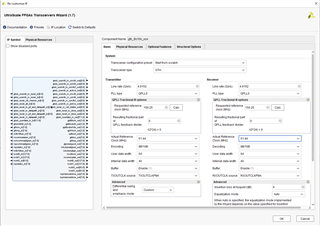
E.g.:

1) Lanerate shoud be 4.9152 Gbps (is it correct?)
2) FPGA ref. clock shoud be 61.44 MHz (but I was not able to reach this value in Latte GUI - error message occured) 
3) Lanes = 2

4) Encoding = 8B10B

5) And what about other parameters? (E, F, K, ...)? 

Configuration script: TI_IP_5Gbps_DDC48.py

Thanks for your advice.

  • Hi Tomas,

    I reviewed the script that you shared and it looks like the AFE is not configured for 64b66b encoding, can you confirm that you are planning to use 64b66b? If you plan to use 8b19b encoding then I would suggest you use the 8b10b reference design as a starting point. Also, I noticed that the lane rates for the DAC and ADC are not the same. We suggest that the lane rate be the same for both the ADC and DAC. This means that you would need to update the LMFS parameters and interpolation such that the lane rates are the same. If you do not plan to use any DACs then you can disable them in the script and you do not have to worry about the DAC configuration. 

    1. If you are using 8b10b encoding then the lane rate for the ADC will be 4.9152 Gbps. 

    2. The reason that you see this error is that the LMK on the EVM only supports a divider of up to 32. With the VCO set to 2949.12MHz it would only be possible to get 92.16MHz. If you would like to get an output of 61.44MHz you can provide an external reference to the LMK, using J14 LMK_CLK_IN, and set the appropriate LMK parameters in Latte. See the picture below for an input of 983.04MHz to the LMK. (Please note that the external freuqency must also be able to provide the 491.52MHz reference to the AFE)

    ...

    3. The number of lanes for the Rx is 2. 

    4. Your script shows an encoding of 8b10b.

    5. The F parameter for Rx is '8' as shown in the LMFS 14810. In your script you have K set to '16' so your FPGA should match this. The E parameter is not used in 8b10b encoding so you do not have to modify this parameter in Vivado project. 

    Things to change in Latte:

    1. Configure the DAC such that the lane rate matches the ADC or disable them if not used.

    2. Update the LMK clocking parameters to expect an input to J14 so that you can get the 61.44MHz clock.

    Things to change in TI JESD204 IP:

    1. Update the header file to have the updated LMFS parameters.

    2. Update the transceiver IP with the lane rate and used lanes.

    3. Update the data unpacking in the refdesign_rx.sv file. This will need to be updated for the 14810 frame format

    ...

    One thing to note is that we are working on reference designs for LMFS 14810 and a decimation factor of 48. We expect to have these designs done and uploaded by April 28th. 

    Regards,

    David Chaparro 

  • Hi David,

    yes, it it correct- I am planning to use 8b10b encoding (I also think that is the only possible choice for the DDC = 48 with 16bit output resolution).

    I tried to set the same lanerate (LMFS parameters) for the DAC, but there was not impact on my issue.

    All others steps shoud be correct. 


    Good to know that this support is planned by the end of this month - thanks for it. I will be able to compare my design with it or use your reference design as a new starting point in my design. I'm looking forward to it. Please let me know as soon as the reference design becomes available.

    Thanks.

    Have a great weekend!

    Tomas

  • Hi David,

    is there any udpate on this issue? 

    Regards,

    Tomas 

  • Hi ,

    I would like to ask if there is any update on when the reference design will be available. Thank you very much for the information.

    Best Regards,

    Tomas 

  • Hi David,

    still no udpate with the reference design?

    Thanks a lot.

    Tomas

  • Hi Tomas,

    The reference design has been uploaded in the AFE79xx Secure folder. The reference design is called "ZCU102_AFE79xx_8b10b_5Gbps_4Rx" and is located in the reference designs sub-folder. 

    Regards,

    David Chaparro