


##############		Read me			##############
#In HSDC Pro DAC tab, Select AFE79xx_2x2TX_14810; Data Rate = 122.88M
#In HSDC Pro ADC tab, Select AFE79xx_2x2RX_14810; Data Rate = 122.88M

sysParams=AFE.systemParams
sysParams.__init__();sysParams.chipVersion=chipVersion

setupParams.skipFpga = 1 # setup FPGA (TSW14J56) using HSDC Pro
##############		Top Level			##############
sysParams.FRef			= 491.52
sysParams.FadcRx		= 2949.12
sysParams.FadcFb		= 2949.12
sysParams.Fdac			= 2949.12*3
sysParams.externalClockRx=False
sysParams.externalClockTx=False
sysParams.RRFMode		= 0					# RRF 0: 4T4R2F FDD Mode
sysParams.enableDacInterleavedMode=False

##############		Digital Chain		##############

		#####	RX	#####
sysParams.ddcFactorRx	=	[24,24,24,24]			#DDC decimation factor for RX A, B, C and D
sysParams.rxNco0		= 	[[5400,5400],			#Band0, Band1 for RXA
							[500,500],        		#Band0, Band1 for RXB
							[2500,2500],        	#Band0, Band1 for RXC
							[1800,1800]]        	#Band0, Band1 for RXD

		#####	FB	#####
sysParams.ddcFactorFb	=	[6,6]					#DDC decimation factor for FB 1 and 2
sysParams.fbNco0		= 	[500,1800]				#Band0 for FB1 and FB2
sysParams.fbEnable		=	[False,False]

		#####	TX	#####
sysParams.ducFactorTx	=	[72,72,72,72]			#DUC interpolation factor for TX A, B, C and D
sysParams.txNco0		= 	[[5400,5400],			#Band0, Band1 for TXA
							[500,500],        		#Band0, Band1 for TXB
							[2500,2500],        	#Band0, Band1 for TXC
							[1800,1800]]        	#Band0, Band1 for TXD


##############		JESD		##############

		#####	ADC-JESD	#####
sysParams.jesdSystemMode= [0,0]
#sysParams.jesdSystemMode= [1,1]
													#SystemMode 0:	2R1F-FDD						; rx1-rx2-fb -fb
													#SystemMode 1:	1R1F-FDD						; rx -rx -fb -fb
													#SystemMode 2:	2R-FDD							; rx1-rx1-rx2-rx2
													#SystemMode 3:	1R								; rx -rx -rx -rx
													#SystemMode 4:	1F								; fb -fb- fb -fb
													#SystemMode 5:	1R1F-TDD						; rx/fb-rx/fb-rx/fb-rx/fb

sysParams.jesdTxProtocol= [0,0]						# 0 - 8b/10b encoding; 2 - 64b/66b encoding
#sysParams.LMFSHdRx		= ["12410","12410","12410","12410"]
sysParams.LMFSHdRx		= ["24410","24410","24410","24410"]
													# The 2nd and 4th are valid only for jesdSystemMode values in (0,2).
													# For other modes, select 4 converter modes for 1st and 3rd.
sysParams.LMFSHdFb		= ["22210","22210"]

#sysParams.rxJesdTxScr	= [False,False,False,False]
sysParams.rxJesdTxScr	= [True,True,True,True]
sysParams.fbJesdTxScr	= [True,True]
#sysParams.fbJesdTxScr	= [False,False]
sysParams.setIlaParams  = True
sysParams.jesdTxIlaM    = [8,8,2,8,8,2]
sysParams.jesdTxIlaLid  = [0,1,2,3,4,5,6,7]
sysParams.jesdTxIlaL    = [4,4,2,4,4,2]

sysParams.rxJesdTxK		= [8,8,8,8]
sysParams.fbJesdTxK		= [8,8]

sysParams.jesdTxLaneMux	= [0,1,2,3,4,5,6,7]			# Enter which lanes you want in each location.
													# For example, if you want to exchange the first two lines of each 2T,
													#		this should be [[1,0,2,3],[5,4,6,7]]

		#####	DAC-JESD	#####
sysParams.jesdRxProtocol= [0,0]
sysParams.LMFSHdTx		= ["12410","12410","12410","12410"]
#sysParams.LMFSHdTx		= ["44210","44210","44210","44210"]
sysParams.jesdRxLaneMux	= [0,1,2,3,4,5,6,7]
#sysParams.jesdRxLaneMux	= [2,1,0,4,3,5,6,7] #0,1,2,3,4,5,6,7]			# Enter which lanes you want in each location.
													# For example, if you want to exchange the first two lines of each 2R
													#		this should be [[1,0,2,3],[5,4,6,7]]
sysParams.jesdRxRbd		= [3, 3]
#sysParams.jesdRxScr		= [False,False,False,False]
sysParams.jesdRxScr		= [True,True,True,True]
sysParams.jesdRxK		= [8,8,8,8]

		#####	JESD Common	#####

sysParams.jesdABLvdsSync= True
sysParams.jesdCDLvdsSync= True
sysParams.syncLoopBack	= True	#JESD Sync signal is connected to FPGA

##############		GPIO		##############
sysParams.gpioMapping	= {
						'H8': 'ADC_SYNC0',
						'H7': 'ADC_SYNC1',
						'N8': 'ADC_SYNC2',
						'N7': 'ADC_SYNC3',
						'H9': 'DAC_SYNC0',
						'G9': 'DAC_SYNC1',
						'N9': 'DAC_SYNC2',
						'P9': 'DAC_SYNC3',
						'P14': 'GLOBAL_PDN',
						'K14': 'FBABTDD',
						'R6': 'FBCDTDD',
						'H15': ['TXATDD','TXBTDD'],
						'V5': ['TXCTDD','TXDTDD'],
						'E7': ['RXATDD','RXBTDD'],
						'R15': ['RXCTDD','RXDTDD']}

##############		LMK Params		##############
lmkParams.pllEn			= True
#lmkParams.inputClk		= 1474.56 # Valid only when lmkParams.pllEn = False
lmkParams.inputClk		= 491.52 # Valid only when lmkParams.pllEn = False
lmkParams.lmkFrefClk	= True
#setupParams.fpgaRefClk	= 245.76 # Should be equal to LaneRate/40 for TSW14J56
setupParams.fpgaRefClk	= 122.88 # Should be equal to LaneRate/40 for TSW14J56
##############		Logging		##############
logDumpInst.setFileName(ASTERIX_DIR+DEVICES_DIR+r"\Afe79xxPg1.txt")
logDumpInst.logFormat=0x0
logDumpInst.rewriteFile=1
logDumpInst.rewriteFileFormat4=1
device.optimizeWrites=0
device.rawWriteLogEn=1

device.delay_time = 0
#-------------------------------------------------------------------------------------------------#
AFE.deviceBringup()

AFE.TOP.overrideTdd(15,3,15)	# bit-wise; 4R,2F,4T

AFE.JESD.ADCJESD[0].adcRampTestPattern(0,1,1)
AFE.JESD.ADCJESD[0].adcRampTestPattern(1,1,1)

#for i in range(4): AFE.DSA.setRxDsa(i,4)

### ADC Ramp Out
#for i in range(3):
#     AFE.JESD.ADCJESD[0].adcRampTestPattern(i,1,1)
#     AFE.JESD.ADCJESD[1].adcRampTestPattern(i,1,1) #chNo, En, RampInc
Hi David,
I am using AFE7900 EVM with Xilinx Ultrazed Evaluation board (Avnet UltraZed-7EV SOM) Part Number (xczu7ev-fbvb900-1-i).
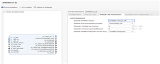
I am programming AFE7900 using latte. The latte script that defines the parameters of AFE7900 are:
ADC Sampling = 2949.12MSPS
L M F S HD = 1 2 4 1 0
sysParams.ddcFactorRx = [24, 24, 24, 24] #DDC decimation factor for RX A, B, C and D decimation by 24
The complete latte python script is attach with the comment
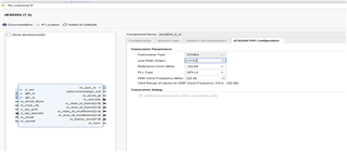
I have using Xilinx AMD IP is for JESD204B receive interface.
Xilinx JESD204 IP’s Parameters
JESD204 Lane rate = 4.9152Gbps
JESD204B interface
Frames per multi-frame = 8
Octet per frame = 4
Lanes in use = 4
Scrambling Enable
Reference Clock = 122.88Mhz
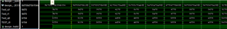
1. When programmed AFE7900 using latte and we have configured our Xilinx JESD204 IP. We get the following logs. I have get the K pattern as expected. Shown in Figure below
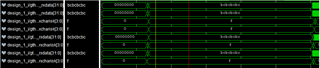
2. Also I get the ILA Pattern as shown below:
3. I have programmed ADC Ramp Pattern Mode in AFE7900 using Latte. I have got the Latte Logs as mentioned below
Writing into 0x0015 value 0x00
Writing into 0x0016 value 0x01
Writing into 0x0109 value 0x02
Writing into 0x0109 value 0x0a
Entered: adcRampTestPattern of class ADCJesdLib
Writing into 0x010a value 0x02
Writing into 0x010a value 0x0a
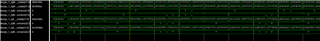
4. I have got the following data on chip-scope for ramp pattern incremented by 2


5. Sync signal that has been given from RTL to AFE7900 is also shown below and the system reference clock frequency is 1.92Mhz

In the above images, I am facing that in ADC ramp pattern i didn't get correct ramp pattern incremented by 2(as expected from Latte configuration file) . Ramp pattern seems in some instance but in most of the time i have seen random numbers or even ramp pattern decremented by 2.
Can you please help me in bringing-up up AFE7900 in this configuration?
Thanks
Umer
