This thread has been locked.

If you have a related question, please click the "Ask a related question" button in the top right corner. The newly created question will be automatically linked to this question.

AFE8000EVM: <--> TSW14J58EVM SYSREF, NOT aligned causing no lane locking

Part Number: AFE8000EVM
Other Parts Discussed in Thread: TSW14J58EVM, AFE8000

eyeIssueLog.txt
AFE80xxCatLibrary
spi - USB Instrument created.
resetDevice
Kintex RegProgrammer - USB Instrument created.
FPGA reset - USB Instrument created.
Power Card - USB Instrument created.
Version : 0x104204b
Connected to Capture Card
Loaded Libraries
Loaded Configuration: AFE8000_SampleConfig.xlsx
Refreshed the GUI.
#================ ERRORS:0, WARNINGS:0 ================#
Programing FPGA ....
Resetting FPGA Pin.
Version : 0x101204c
Connected to Capture Card
FPGA Tx did not capture sysref
FPGA Rx did not capture sysref
Setting RBD to: 11
###########Device DAC JESD-RX 0 Link Status###########
Errors=0b11000000; Got errors: EoMB alignment error; EoEMB alignment error; 
Comma Align Lock Lane0: False; Please check if the transmitter is sending data and eye is good.
Comma Align Lock Lane1: False; Please check if the transmitter is sending data and eye is good.
Comma Align Lock Lane2: False; Please check if the transmitter is sending data and eye is good.
Comma Align Lock Lane3: False; Please check if the transmitter is sending data and eye is good.
CS State TX0: 0b00000000 . It is expected to be 0b10101010
BUF State TX0: 0b00000000 . It is expected to be 0b11111111
Couldn't get the link up for device RX: 0
###################################
DAC Start

Hello,

hardware: AFE8000EVM <--> DC182 TSW14J58 

POWER:
AFE8000EVM 12DC (4A limited)

DC182 TSW14J58 5VDC(5A limited)

INPUT SIG:

10MHz 10dBm from sig gen to AFE8000EVM J18 LMK_CLKIN

OUTPUT SIG:

SMA connector to AFE8000EVM J13 TXA_OUT

CONTROL:

2x USB DC182 TSW14j58evm (1 is SS USB and is connected to an adequate SS Port on the computer)

1x USB AFE8000EVM

Please note that the DC182 TSW14j58EVM has had the firmware updated to the JESD204C version.

SOFTWARE:

AFE80xxCat.Exe

I am following the steps in the AFE8000EVM_Bringup_Guide power point and I am receiving errors at step 6, the errors are in the attached "eyeIssueLog.txt" file.

1) How do I check if the sysref is being captured on the Tx and Rx sides.

2) How do I check if the transmitter is sending data and the eye is good?

Thank you in advance.

  • Hi Oliver,

    Looking at the log you posted, it looks like it is incomplete. Let me ask you a couple of questions:

    1. Is that the complete log? Because at no point is it programming the AFE8000.
    2. Are you sure you have the jumper J35 of the TSW14j58EVM in the 1-2 position before powering up the board? The reason why I ask this is because I can see the FPGA firmware reported change from version 0x104204b to 0x101204c.
    3. Did you click the "Device Bringup" button in step 3 of the bringup guide?

    Best,

    Camilo

  • Hi Camilo,

    Thank you for responding.

    1 & 3) It was the complete log but for some reason I was under the impression the Device Bringup" happened when the parameters were loaded so didn't need to be clicked.

    2) I have checked that the jumper is in position 1-2 for J35

    I have re-run the system checking everything you mentioned checking the power supply is correct and the RF signal input is correct (10MHz, +10dBm).

    The new log file (Log2.txt) is attached with a similar issue, it is worth noting that the AFE80XXCat program does go into a (not responding) status each time I run the "Device Bringup". 

    Log2.txt
    AFE80xxCatLibrary
    spi - USB Instrument created.
    resetDevice
    Kintex RegProgrammer - USB Instrument created.
    Kintex RegProgrammer - USB Instrument created.
    Kintex RegProgrammer - USB Instrument created.
    FPGA reset - USB Instrument created.
    Power Card - USB Instrument created.
    Version : 0x101204c
    Connected to Capture Card
    Loaded Libraries
    Loaded Configuration: AFE8000_SampleConfig.xlsx
    Refreshed the GUI.
    #================ ERRORS:0, WARNINGS:0 ================#
    Loaded Configuration: AFE8000_SampleConfig.xlsx
    Refreshed the GUI.
    Device Initialization for ChipVersion: 2.0
    The External Sysref Frequency should be an integer factor of: 3.90625MHz
    2T2R1F Number: 0
    Valid Configuration: True
    laneRateRx: 24750.0
    laneRateRx1: 24750.0
    laneRateFb: 24750.0
    laneRateTx0: 24750.0
    laneRateTx1: 24750.0
    2T2R1F Number: 1
    Valid Configuration: True
    laneRateRx: 24750.0
    laneRateRx1: 24750.0
    laneRateFb: 24750.0
    laneRateTx0: 24750.0
    laneRateTx1: 24750.0
    LMK Clock Divider - Device registers reset.
    LMK Clock Divider - Device registers reset.
    REFCLOCK is used from LMK source, ensure board connections are ok to do the same
    LMK and FPGA Configured.
    DONOT_OPEN_Afe80xx_FULL - Device registers reset.
    chipType: 0xa
    chipId: 0x8001
    chipVersion: 0x20
    Programing FPGA ....
    Resetting FPGA Pin.
    Version : 0x101204c
    Connected to Capture Card
    Resetting FPGA.
    Version : 0x101204c
    Connected to Capture Card
    LMK and FPGA Configured.
    AFE Reset Done
    Fuse farm load autoload done successful
    No autload error
    Fuse farm load autoload done successful
    No autload error
    //Firmware Version = 9108
    //PG Version = 1
    //Release Date [dd/mm/yy] = 28/8/20
    //Patch Version = 0
    //PG Version = 0
    //Release Date [dd/mm/yy] = 0/0/0
    AFE MCU Wake up done and patch loaded.
    PLL Locked
    AFE PLL Configured.
    AFE SerDes Configured.
    AFE Digital Chains configured.
    AFE TX Analog configured.
    AFE RX Analog configured.
    AFE FB Analog configured.
    AFE JESD configured.
    AFE AGC configured.
    AFE PAP and Alarms configured.
    AFE GPIO configured.
    Sysref Read as expected
    FPGA Tx sysref captured
    FPGA Rx sysref captured
    FPGA Tx sysref captured
    FPGA Rx sysref captured
    Setting RBD to: 11
    Setting RBD to: 11
    FPGA Tx sysref captured
    FPGA Rx sysref captured
    FPGA Tx sysref captured
    FPGA Rx sysref captured
    Setting RBD to: 11
    ###########Device DAC JESD-RX 0 Link Status###########
    CS State TX0: 0b00000000 . It is expected to be 0b10101010
    BUF State TX0: 0b00000000 . It is expected to be 0b11111111
    Couldn't get the link up for device RX: 0
    ###################################
    ###########Device DAC JESD-RX 1 Link Status###########
    Comma Align Lock Lane3: False; Please check if the transmitter is sending data and eye is good.
    CS State TX0: 0b00000000 . It is expected to be 0b10101010
    BUF State TX0: 0b00000000 . It is expected to be 0b11111111
    Couldn't get the link up for device RX: 1
    ###################################
    AFE Configuration Complete
    #================ ERRORS:3, WARNINGS:0 ================#
     

    The positions of the other Jumpers on the TSW14J58EVM are:

    (other J values have no jumper attached)

    J21 1-2
    J29 1-2
    J30 1-2
    J34 2-3
    J35 1-2

    I notice that the RBD values do not match, could you provide some insight into what they represent?

    Thank you for the help!

    Kind regards

    Oliver Forbes-Shaw

  • Hi Oliver,

    From the log you have posted I can see that your JESD link is not coming up and since the CS state is 0b00 it means it is not seeing the K characters. Could you please try the following:

    1. In the "Command Line" window after the Device Bringup finishes could you use the command "AFE.adcDacSync(1)"
    2. Could you make sure that the FMC connection between the AFE8000 and the TSW14J58 is secure? We have had people not press it all the way in.

    For the RBD values, do you mean that the values are not the same every bringup?

    Best,

    Camilo

  • AFE8000EVMlog3.txt
    AFE80xxCatLibrary
    spi - USB Instrument created.
    resetDevice
    Kintex RegProgrammer - USB Instrument created.
    Kintex RegProgrammer - USB Instrument created.
    Kintex RegProgrammer - USB Instrument created.
    FPGA reset - USB Instrument created.
    Power Card - USB Instrument created.
    Version : 0x101204c
    Connected to Capture Card
    Loaded Libraries
    Loaded Configuration: AFE8000_SampleConfig.xlsx
    Refreshed the GUI.
    #================ ERRORS:0, WARNINGS:0 ================#
    Loaded Configuration: AFE8000_SampleConfig.xlsx
    Refreshed the GUI.
    Device Initialization for ChipVersion: 2.0
    The External Sysref Frequency should be an integer factor of: 3.90625MHz
    2T2R1F Number: 0
    Valid Configuration: True
    laneRateRx: 24750.0
    laneRateRx1: 24750.0
    laneRateFb: 24750.0
    laneRateTx0: 24750.0
    laneRateTx1: 24750.0
    2T2R1F Number: 1
    Valid Configuration: True
    laneRateRx: 24750.0
    laneRateRx1: 24750.0
    laneRateFb: 24750.0
    laneRateTx0: 24750.0
    laneRateTx1: 24750.0
    LMK Clock Divider - Device registers reset.
    LMK Clock Divider - Device registers reset.
    REFCLOCK is used from LMK source, ensure board connections are ok to do the same
    LMK and FPGA Configured.
    DONOT_OPEN_Afe80xx_FULL - Device registers reset.
    chipType: 0xa
    chipId: 0x8001
    chipVersion: 0x20
    Programing FPGA ....
    Resetting FPGA Pin.
    fpgaResetFtdi._pin0 : write failed.
    fpgaResetFtdi._pin0 : write failed.
    Version : 0x0
    Could not connect to capture card. Reset Card and Reconnect( myfpga.Reconnect() )
    Resetting FPGA.
    Version : 0x101204c
    Connected to Capture Card
    LMK and FPGA Configured.
    AFE Reset Done
    Fuse farm load autoload done successful
    No autload error
    Fuse farm load autoload done successful
    No autload error
    //Firmware Version = 9108
    //PG Version = 1
    //Release Date [dd/mm/yy] = 28/8/20
    //Patch Version = 0
    //PG Version = 0
    //Release Date [dd/mm/yy] = 0/0/0
    AFE MCU Wake up done and patch loaded.
    PLL Locked
    AFE PLL Configured.
    AFE SerDes Configured.
    AFE Digital Chains configured.
    AFE TX Analog configured.
    AFE RX Analog configured.
    AFE FB Analog configured.
    AFE JESD configured.
    AFE AGC configured.
    AFE PAP and Alarms configured.
    AFE GPIO configured.
    Sysref Read as expected
    FPGA Tx did not capture sysref
    FPGA Rx did not capture sysref
    FPGA Tx did not capture sysref
    FPGA Rx did not capture sysref
    Setting RBD to: 11
    Setting RBD to: 11
    FPGA Tx did not capture sysref
    FPGA Rx did not capture sysref
    FPGA Tx did not capture sysref
    FPGA Rx did not capture sysref
    Setting RBD to: 11
    ###########Device DAC JESD-RX 0 Link Status###########
    CS State TX0: 0b00000000 . It is expected to be 0b10101010
    BUF State TX0: 0b00000000 . It is expected to be 0b11111111
    Couldn't get the link up for device RX: 0
    ###################################
    ###########Device DAC JESD-RX 1 Link Status###########
    CS State TX0: 0b00000000 . It is expected to be 0b10101010
    BUF State TX0: 0b00000000 . It is expected to be 0b11111111
    Couldn't get the link up for device RX: 1
    ###################################
    AFE Configuration Complete
    #================ ERRORS:11, WARNINGS:2 ================#
    FPGA Tx did not capture sysref
    FPGA Rx did not capture sysref
    ###########Device DAC JESD-RX 0 Link Status###########
    CS State TX0: 0b00000000 . It is expected to be 0b10101010
    BUF State TX0: 0b00000000 . It is expected to be 0b11111111
    Couldn't get the link up for device RX: 0
    ###################################
    ###########Device DAC JESD-RX 1 Link Status###########
    CS State TX0: 0b00000000 . It is expected to be 0b10101010
    BUF State TX0: 0b00000000 . It is expected to be 0b11111111
    Couldn't get the link up for device RX: 1
    ###################################
    #======
    AFE8000EVMlog4.txt
    AFE80xxCatLibrary
    spi - USB Instrument created.
    resetDevice
    Kintex RegProgrammer - USB Instrument created.
    Kintex RegProgrammer - USB Instrument created.
    Kintex RegProgrammer - USB Instrument created.
    FPGA reset - USB Instrument created.
    Power Card - USB Instrument created.
    Version : 0x101204c
    Connected to Capture Card
    Loaded Libraries
    Loaded Configuration: AFE8000_SampleConfig.xlsx
    Refreshed the GUI.
    #================ ERRORS:0, WARNINGS:0 ================#
    Loaded Configuration: AFE8000_SampleConfig.xlsx
    Refreshed the GUI.
    Device Initialization for ChipVersion: 2.0
    The External Sysref Frequency should be an integer factor of: 3.90625MHz
    2T2R1F Number: 0
    Valid Configuration: True
    laneRateRx: 24750.0
    laneRateRx1: 24750.0
    laneRateFb: 24750.0
    laneRateTx0: 24750.0
    laneRateTx1: 24750.0
    2T2R1F Number: 1
    Valid Configuration: True
    laneRateRx: 24750.0
    laneRateRx1: 24750.0
    laneRateFb: 24750.0
    laneRateTx0: 24750.0
    laneRateTx1: 24750.0
    LMK Clock Divider - Device registers reset.
    LMK Clock Divider - Device registers reset.
    REFCLOCK is used from LMK source, ensure board connections are ok to do the same
    LMK and FPGA Configured.
    DONOT_OPEN_Afe80xx_FULL - Device registers reset.
    chipType: 0xa
    chipId: 0x8001
    chipVersion: 0x20
    Programing FPGA ....
    Resetting FPGA Pin.
    Version : 0x101204c
    Connected to Capture Card
    Resetting FPGA.
    Version : 0x0
    Could not connect to capture card. Reset Card and Reconnect( myfpga.Reconnect() )
    Mismatch in the FPGA bit file version. AFE JESD Protocol is 204C but the FPGA bit file is 0x0
    LMK and FPGA Configured.
    AFE Reset Done
    Fuse farm load autoload done successful
    No autload error
    Fuse farm load autoload done successful
    No autload error
    //Firmware Version = 9108
    //PG Version = 1
    //Release Date [dd/mm/yy] = 28/8/20
    //Patch Version = 0
    //PG Version = 0
    //Release Date [dd/mm/yy] = 0/0/0
    AFE MCU Wake up done and patch loaded.
    PLL Locked
    AFE PLL Configured.
    AFE SerDes Configured.
    AFE Digital Chains configured.
    AFE TX Analog configured.
    AFE RX Analog configured.
    AFE FB Analog configured.
    AFE JESD configured.
    AFE AGC configured.
    AFE PAP and Alarms configured.
    AFE GPIO configured.
    Sysref Read as expected
    FPGA Tx sysref captured
    FPGA Rx sysref captured
    FPGA Tx sysref captured
    FPGA Rx sysref captured
    Setting RBD to: 11
    Setting RBD to: 11
    FPGA Tx sysref captured
    FPGA Rx sysref captured
    Programing FPGA ....
    Resetting FPGA Pin.
    fpgaResetFtdi._pin0 : write failed.
    fpgaResetFtdi._pin0 : write failed.
    Version : 0xdec0de1cL
    Could not connect to capture card. Reset Card and Reconnect( myfpga.Reconnect() )
    FPGA Tx did not capture sysref
    FPGA Rx did not capture sysref
    Setting RBD to: 11
    ###########Device DAC JESD-RX 0 Link Status###########
    CS State TX0: 0b00000000 . It is expected to be 0b10101010
    BUF State TX0: 0b00000000 . It is expected to be 0b11111111
    Couldn't get the link up for device RX: 0
    ###################################
    ###########Device DAC JESD-RX 1 Link Status###########
    CS State TX0: 0b00000000 . It is expected to be 0b10101010
    BUF State TX0: 0b00000000 . It is expected to be 0b11111111
    Couldn't get the link up for device RX: 1
    ###################################
    AFE Configuration Complete
    #================ ERRORS:7, WARNINGS:2 ================#
    Device Initialization for ChipVersion: 2.0
    The External Sysref Frequency should be an integer factor of: 3.90625MHz
    2T2R1F Number: 0
    Valid Configuration: True
    laneRateRx: 24750.0
    laneRateRx1: 24750.0
    laneRateFb: 24750.0
    laneRateTx0: 24750.0
    laneRateTx1: 24750.0
    2T2R1F Number: 1
    Valid Configuration: True
    laneRateRx: 24750.0
    laneRateRx1: 24750.0
    laneRateFb: 24750.0
    laneRateTx0: 24750.0
    laneRateTx1: 24750.0
    LMK Clock Divider - Device registers reset.
    LMK Clock Divider - Device registers reset.
    REFCLOCK is used from LMK source, ensure board connections are ok to do the same
    LMK and FPGA Configured.
    DONOT_OPEN_Afe80xx_FULL - Device registers reset.
    chipType: 0xa
    chipId: 0x8001
    chipVersion: 0x20
    Programing FPGA ....
    Resetting FPGA Pin.
    Version : 0x101204c
    Connected to Capture Card
    Resetting FPGA.
    Version : 0x101204c
    Connected to Capture Card
    LMK and FPGA Configured.
    AFE Reset Done
    Fuse farm load autoload done successful
    No autload error
    Fuse farm load autoload done successful
    No autload error
    //Firmware Version = 9108
    //PG Version = 1
    //Release Date [dd/mm/yy] = 28/8/20
    //Patch Version = 0
    //PG Version = 0
    //Release Date [dd/mm/yy] = 0/0/0
    AFE MCU Wake up done and patch loaded.
    PLL Locked
    AFE PLL Configured.
    AFE SerDes Configured.
    AFE Digital Chains configured.
    AFE TX Analog configured.
    AFE RX Analog configured.
    AFE FB Analog configured.
    AFE JESD configured.
    AFE AGC configured.
    AFE PAP and Alarms configured.
    AFE GPIO configured.
    Sysref Read as expected
    FPGA Tx sysref captured
    FPGA Rx sysref captured
    FPGA Tx sysref captured
    FPGA Rx sysref captured
    Setting RBD to: 11
    Setting RBD to: 11
    FPGA Tx sysref captured
    FPGA Rx sysref captured
    FPGA Tx sysref captured
    FPGA Rx sysref captured
    Setting RBD to: 11
    ###########Device DAC JESD-RX 0 Link Status###########
    CS State TX0: 0b00000000 . It is expected to be 0b10101010
    BUF State TX0: 0b00000000 . It is expected to be 0b11111111
    Couldn't get the link up for device RX: 0
    ###################################
    ###########Device DAC JESD-RX 1 Link Status###########
    CS State TX0: 0b00000000 . It is expected to be 0b10101010
    BUF State TX0: 0b00000000 . It is expected to be 0b11111111
    Couldn't get the link up for device RX: 1
    ###################################
    AFE Configuration Complete
    #================ ERRORS:2, WARNINGS:0 ================#
    #Error: 'afeLibrary' object has no attribute 'adcSync'
    # "", line 1, in 
    # AttributeError: 'afeLibrary' object has no attribute 'adcSync'
    # 
    # 
    #================ ERRORS:1, WARNINGS:0 ================#
    FPGA Tx sysref captured
    FPGA Rx sysref captured
    ###########Device DAC JESD-RX 0 Link Status###########
    CS State TX0: 0b00000000 . It is expected to be 0b10101010
    BUF State TX0: 0b00000000 . It is expected to be 0b11111111
    Couldn't get the link up for device RX: 0
    ###################################
    ###########Device DAC JESD-RX 1 Link Status###########
    CS State TX0: 0b00000000 . It is expected to be 0b10101010
    BUF State TX0: 0b00000000 . It is expected to be 0b11111111
    Couldn't get the link up for device RX: 1
    ###################################
    #======

    Hi Camillo,

    I connected up the boards and double checked the connection was tight.

    I have ran the Bring up process twice (Everything was powered down and reset buttons pressed between each bring up process being ran) and ran the command "AFE.adcDacSync(1)" both times as requested.

    the Log files are attached, I have also attached the settings for the card when the detect hardware button is pressed in case that is a cause.

    Cheers in advance.

  • Hi Oliver,

    Ok, here are a few questions and things to try:

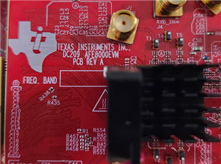
    1. The AFE EVM you have does say “DC209 AFE8000EVM” like in the picture below correct?


    1. After you finish the bringup, could you skip steps 5-7 and follow steps 8 – 10 to see if you can capture with the RX channels?
    2. I understand you said you are using a 5V 5A for the TSW14J58, could you check that the voltage at the header jack is 5V with a multimeter. Sometimes with the cables we have had to increase the power supply to around 5.5V to account for the loss.
    3. Could you try to run the following three commands in Command Line after bringup? These are to recalculate the RBD.

    AFE.JESD.DACJESD[0].setGoodRbd()
    AFE.JESD.DACJESD[1].setGoodRbd()
    AFE.adcDacSync(1)

    Best,

    Camilo

  • Hi Camilo,

    1) I can confirm the board does state "DC209 AFE8000EVM" (this did confuse me also regarding the detect board)

    3) I have checked the voltage and it is 5.012VDC at the connection jack but I have upped the power supply to 5.5VDC.

    I tried the "bringup" after changing the "AFE_BOARD_TYPE"  to the "DC209" with the voltage increase and it did work on the 3rd attempt start to finish, I am not sure on the Stability as in if it completes bring up every time as yet.

    This does prove that the hardware works but I just want to make sure that it works every time now.

    I am still not sure why the detect hardware button does detects the board type as the "HSC1463" as yet.

    Is there any other information you need me to provide of this anomaly? 

  • Hi Oliver,

    From the logs you have provided I see that the AFE8000 gets programmed every time, it just looked like there were some problems when stablishing the JESD link which is odd. If you still see stability issues please try running the 3 lines below:

    AFE.JESD.DACJESD[0].setGoodRbd()
    AFE.JESD.DACJESD[1].setGoodRbd()
    AFE.adcDacSync(1)

    To fix the handle of the AFE8000EVM that is detected by the GUI you can follow the steps on this guide and download the FT_PROG program from the link below. I am also attaching the FTDI template.

    https://ftdichip.com/utilities/ 

    AFE8000-EVM-Program-FTDI-Handle.docx

    AFE8000- FTDI_TEMPLATE_RevA.xml
    <?xml version="1.0" encoding="utf-16"?>
    <FT_EEPROM>
      <Chip_Details>
        <Type>FT4232H</Type>
      </Chip_Details>
      <USB_Device_Descriptor>
        <VID_PID>0</VID_PID>
        <idVendor>0403</idVendor>
        <idProduct>6011</idProduct>
        <bcdUSB>USB 2.0</bcdUSB>
      </USB_Device_Descriptor>
      <USB_Config_Descriptor>
        <bmAttributes>
          <RemoteWakeupEnabled>false</RemoteWakeupEnabled>
          <SelfPowered>false</SelfPowered>
          <BusPowered>true</BusPowered>
        </bmAttributes>
        <IOpullDown>false</IOpullDown>
        <MaxPower>100</MaxPower>
      </USB_Config_Descriptor>
      <USB_String_Descriptors>
        <Manufacturer>FTDI</Manufacturer>
        <Product_Description>AFE8000_DC209_RevA</Product_Description>
        <SerialNumber_Enabled>true</SerialNumber_Enabled>
        <SerialNumber />
        <SerialNumberPrefix>FT</SerialNumberPrefix>
        <SerialNumber_AutoGenerate>true</SerialNumber_AutoGenerate>
      </USB_String_Descriptors>
      <Hardware_Specific>
        <TPRDRV>0</TPRDRV>
        <Port_A>
          <VCP>true</VCP>
          <D2XX>false</D2XX>
          <RI_RS485>false</RI_RS485>
        </Port_A>
        <Port_B>
          <VCP>true</VCP>
          <D2XX>false</D2XX>
          <RI_RS485>false</RI_RS485>
        </Port_B>
        <Port_C>
          <VCP>true</VCP>
          <D2XX>false</D2XX>
          <RI_RS485>false</RI_RS485>
        </Port_C>
        <Port_D>
          <VCP>true</VCP>
          <D2XX>false</D2XX>
          <RI_RS485>false</RI_RS485>
        </Port_D>
        <IO_Pins>
          <Group_A>
            <SlowSlew>false</SlowSlew>
            <Schmitt>false</Schmitt>
            <Drive>4mA</Drive>
          </Group_A>
          <Group_B>
            <SlowSlew>false</SlowSlew>
            <Schmitt>false</Schmitt>
            <Drive>4mA</Drive>
          </Group_B>
          <Group_C>
            <SlowSlew>false</SlowSlew>
            <Schmitt>false</Schmitt>
            <Drive>4mA</Drive>
          </Group_C>
          <Group_D>
            <SlowSlew>false</SlowSlew>
            <Schmitt>false</Schmitt>
            <Drive>4mA</Drive>
          </Group_D>
        </IO_Pins>
      </Hardware_Specific>
    </FT_EEPROM>

    However, the problem on the link should not be related to the name.

    Best,

    Camilo

  • Thank you for all the help Camilo, I will try this in the Morning

  • Understood. 

    Best,

    Camilo

  • Good Morning Camilo,

    I tried the USB fix and it now recognises the board as the correct "AFE8000_DC209_RevA" so thank you for that.

    I have tried the fix for getting the Tx and Rx links up via the commands you specified and that seems to work.
    I do need to use this command consistently though soi have made a note of it.

    Kind regards 

    Oliver Forbes-Shaw

  • Understood, no problem.

    Best,

    Camilo