This thread has been locked.

If you have a related question, please click the "Ask a related question" button in the top right corner. The newly created question will be automatically linked to this question.

TRF3705: Is it possible to drive TRF3705 BB inputs directly from a FPGA ?

Part Number: TRF3705
Other Parts Discussed in Thread: THS4513

Dear Team,

My customer would like to create a simple BPSK/QPSM modulation using an IQ modulator like the TRF3705.

They would like to drive the BBIP/N and BBQP/N directly from an FPGA using a digital output.

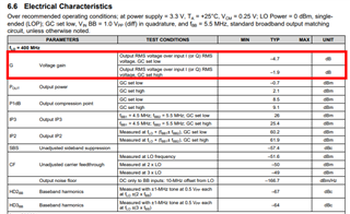
Since the input impedance of the BB inputs are 8Kohm we don't expect it will load the FPGA.

  1. Is it possible to do using the TRF3705 ?
  2. Do we have an alternative part number we can advise for such operation mode ?
    Main system spec are low power mode and fast wakeup/standby mode


Would anyone on your team be able to advise ?

Regards,

Nir.

  • Nir,

    The TRF3705 baseband input are biased at 0.5V VCM maximum. Therefore, driving CMOS signal with level of 1.8V is not feasible. 

    I am adding Russell to chime in as well. In general, FPGA CMOS signal has lots of noise and harmonics, and customer should not expect good performance coming out of the TRF3705.

    -Kang

  • Hi,

    Please explain why low Vcm cause difficult to drive CMOS signals

    Regards,

    Marco

  • Marco,

    The TRF3705 requires VCM external bias of 0.25V to 0.5V for optimal OIP3 performance. This is by design to interface seamlessly with our DAC348x products. Any bias of the baseband input greater than 0.5V will start saturating the baseband amplifier, and causing degradation (and potential damage) to the TRF3705 baseband amplifier input. 

  • Hi,

    If the drived signal will be 3.3V instead of 1.8V it will better?

  • Hi Marco,

    If the drived signal will be 3.3V instead of 1.8V it will better?

    No, if the logic level is at 3.3V, the common mode for the 3.3V logic is actually higher at 3.3/2 = 1.65V. This is higher than the 1.8V VCM of 0.9V. Therefore, you would actually get worse RF performance for 3.3V logic.

    -Kang

  • Hi Kang,

    We're a bit puzzled here.

    We want to work with digital signals '0' and '1' in order to create a BPSK/QPSK modulation.

    1. Is it possible ?

    2. What should be the appropriate voltage levels for the '0' and the '1' in this case

    We can also use a buffer between the FPGA and the modulator if needed.

    Regards,

    Nir

  • Nir,

    You will need a DAC to interface between the FPGA and the TRF3705. You cannot drive a straight logic level into the TRF3705 as logic drivers are not meant to be good analog interface driver. See examples:

    https://www.ti.com/lit/ug/slua647a/slua647a.pdf

    -Kang

  • Hi Kang,

    Thanks for the reference to the app-note.

    While I understand the need for the analog interfacing network, I'm not sure I understand why the modulation waveform should only come from a DAC and not from any other digital device FPGA/MCU etc ?

    If we use the right filtering from the FPGA to the modulator and proper interfacing network do you see any reason why it won't work ?

    Is it something anyone on the team will be able to check ?
    For example using MSPM0/C2000 as a simple modem or even only a PWM generator --> Interfacing network --> to drive the TRF3705.

    Regards,

    Nir.

  • Nir,

    For simple BPSK, you can design the level shifter circuit to reduce the amplitude of the CMOS output to appropriate bias level of 0.5V VCM with the proper swing, and I agree you can achieve the interface requirement.

    The design of the TRF3705 has to accommodate higher order QAMs such as 1024 QAM, and the use of BPSK in a bit level is not possible, and only the DAC can achieve the 1024 QAM performance. For example, a 64 QAM requires 8 levels of amplitude. I cannot see FPGA CMOS output to be able to drive 8 different levels of amplitude correctly.

    The application note mentioned above should provide sufficient points for you to design the level translators to interface between the CMOS driver and the TRF3705. The CMOS driver will have low output impedance and is a voltage based driver. You should be able to design a two component resistor divider to achieve this.

    Please note that I still cannot see how you can drive the TRF3705 differentially. Driving the TRF3705 differentially is essential to the RF performance.

    -Kang

  • Hi Kang,

    Since the modulation we're looking into is a simple BPSK or 4QAM we can work with '0', and '1' for each I/Q.

    We're currently looking into using a FDA like THS4513 as an FDA + differential LPF in order to set up the Vcm=0.25V and input voltages correctly.

    Would you or anyone on the team comment on the Max and Min voltages allowed on the BBIP/BBIM/BBQP/BBQM pins ?

    If the VinBB is 1Vpp with common mode voltage of 0.25V does it means that the actual voltages we should plan are -0.25V to +0.75V. Did we understand this correctly ?

    Regards,

    Nir

  • Nir,

    The voltage input depends on the output power requirement at the TRF3705 output. This is gain and frequency dependent. You may back calculate by:

    1. Refer to section 6.6 below.

    2. allocate the gain vs. frequency information

    3. Based on the TRF3705 output Pout requirement, back calculate the RMS input through the gain specified.

    The RMS input can be then converted to peak to peak voltage. The peak to peak will be centered at 0.25V common mode.

    The max Pout of the TRF3705 should not exceed the P1dB

    -Kang