This thread has been locked.

If you have a related question, please click the "Ask a related question" button in the top right corner. The newly created question will be automatically linked to this question.

AFE8000EVM: Bringup with VPK120 FPGA board

Part Number: AFE8000EVM
Other Parts Discussed in Thread: LMK04828, AFE8000

I'm bring up the AFE8000EVM board, matched with the VPK120 board from Xilinx.

Synthesis of the FPGA using the reference design you provided seems to work.

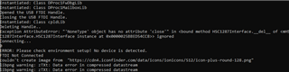
However when I download the image to the FPGA using vivado, I see the following messages:


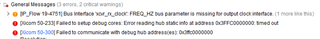
I think the image is being loaded correctly - I've added some debug logic and that seems ok, but I don't know why I'm seeing these error messages.

Further debug suggests that the FPGA isn't receiving a clock from the AFE8000EVM, and it is being held in reset.

Looking at the AFE8000EVM board, when I try to connect to Latte I see the following at boot time:

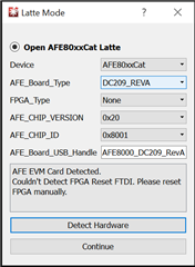
The message suggests it can see the EVM card, but not the FPGA. I'm not sure if this is as a result of the configuration issues.

When I press "Continue" in Latte I see the following messages in the main GUI:

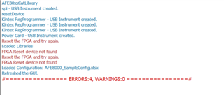
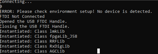
and these are the interesting parts of the console log:

Any assistance you can give here will be very helpful.

Other than that I have a couple of specific questions:

What is the required configuration order. 

Do I need to have the FPGA programmed successfully before running Latte? If so, is the lack of a clock a problem?

Alternatively do I need to access Latte to allow it to program the LMK04828 before I configure the FPGA?

Can you confirm what clock frequency I need to supply to LMK_CLKIN? In the documentation supplied with the 

release (RefDesign-Doc.pptx) there are references to 968MHz, but in the AFE8000EVMBringupGuide.pptx it suggests 10MHz.

We think the 10MHz is correct, but can you confirm?

  • Hi Philip,

    The errors you are seeing in Vivado may be related to the first board change i mention below. Please check that this change has been made. 

    The FPGA reset errors in the Latte software are expected and can be ignored.

    After looking at the EVM I noticed that there are two board modifications that are reqrueid in order for the reference design to work. Can you check if these have been made on your board?

    1. R487 should be removed. 

    2. One of the JESD clocks from the LMK may not be connected and the below changes should be made to resistors R318 and R321

    The proper bringup sequence is to first program the LMK on the AFE EVM then program the FPGA. The clocks to the FPGA should be stable before loading the FPGA firmware. 

    The correct clock is 968MHz, as mentioned in the setup document. Please note that the BringupGuide is for the example configuration only and should not be followed for this reference design. The steps outlined in page 14 of the 'RefDesign-Doc.pptx' document should be followed.

    Regards,

    David Chaparro

  • Hi David.

    Thanks a lot for your response. I've made significant progress now. I note however that the RefDesign-Doc.pptx seems to be incorrect.

    On Page 14 it states:

    1.Program FPGA with bitfiles

    2.Source vivado_hw_scripts.tcl in Vivado

          1.This will set up all the VIO probe names and activate all resets

    3.Program EVM clocking through AFE80xxCat GUI

         1.Browse and Load ‘AFE8000_32Gbps.xlsx”

          2.Enter the GUI script mode, by pressing Ctrl+Shift+S, and run ConfigLmk.py

    But I think what is shows as step 1 - Program FPGA, should come after steps two and three.

    I'm not completely there, however. I'm seeing the following at the end of my Latte log:

    AFE MCU Wake up done and patch loaded.

    PLL Locked

    AFE PLL Configured.

    AFE SerDes Configured.

    AFE Digital Chains configured.

    AFE TX Analog configured.

    AFE RX Analog configured.

    AFE FB Analog configured.

    AFE JESD configured.

    AFE AGC configured.

    AFE PAP and Alarms configured.

    AFE GPIO configured.

    Sysref Read as expected

    Setting RBD to: 11

    Setting RBD to: 11

    Setting RBD to: 11

    ###########Device DAC JESD-RX 0 Link Status###########

    Comma Align Lock Lane0: False; Please check if the transmitter is sending data and eye is good.

    Comma Align Lock Lane1: False; Please check if the transmitter is sending data and eye is good.

    Comma Align Lock Lane2: False; Please check if the transmitter is sending data and eye is good.

    Comma Align Lock Lane3: False; Please check if the transmitter is sending data and eye is good.

    CS State TX0: 0b00000000 . It is expected to be 0b10101010

    BUF State TX0: 0b00000000 . It is expected to be 0b11111111

    Couldn't get the link up for device RX: 0

    ###################################

    ###########Device DAC JESD-RX 1 Link Status###########

    Comma Align Lock Lane0: False; Please check if the transmitter is sending data and eye is good.

    Comma Align Lock Lane1: False; Please check if the transmitter is sending data and eye is good.

    Comma Align Lock Lane2: False; Please check if the transmitter is sending data and eye is good.

    Comma Align Lock Lane3: False; Please check if the transmitter is sending data and eye is good.

    CS State TX0: 0b00000000 . It is expected to be 0b10101010

    BUF State TX0: 0b00000000 . It is expected to be 0b11111111

    Couldn't get the link up for device RX: 1

    ###################################

    AFE Configuration Complete

    #================ ERRORS:10, WARNINGS:0 ================#

    It seems like the JESD links aren't going, with the ILA in the FPGA containing all zeros.

    Do you have any further suggestions?

  • Hi Philip,

    The steps 1-3 are in the correct order and should not be the cause of the issue you are seeing. One thing to check is that after running the ConfigLmk script are you setting the master_reset and tx_reset inactive before running ConfigAFE? If the Tx is not taken out of reset then the FPGA will not be sending data to the DAC and the error that you are seeing could occur. 

    Regards,

    David Chaparro 

  • Hi David,

    I'm pretty sure the steps 1-3 are wrong in the document.

    If I follow them as described Vivado returns the error messages I attached to my original post (and a popup), the ILA and VIO windows don't appear and the vivado_hw_scripts.tcl script fails with lots of naming problems as the VIOs aren't setup correctly.

    The document also doesn't agree with your earlier comment:

    "The proper bringup sequence is to first program the LMK on the AFE EVM then program the FPGA"

    I've had to change the order to get the FPGA to finish configuration and the associated checks.

    Separately I've added some debug to the FPGA and routed some signals to a logic analyser.

    This allows me to see that

    1) The FPGA transmit path is active. I see the tx data into the jesd_ip_inst toggling and the tx_start_of_emblock signal pulsing occasionally.

    2) No activity is seen on the FPGA out of the JESD on the RX path. This matches with the ILA always containing 0s (and me having to manually trigger it)

    I've tried running the ADC capture feature as described in section 7 of the Latte user guide, but it appears something is going wrong there. When I click on the 'Start' button it turns to an error and I see:

    #=============ERRORS:1, WARNINGS:0

    58WrapperClass instance has no attribute 'printCommentsForDebug'

    No values received from capture Device

    process.bitFunctions - Error in computing bitFunctions block. Check if all values are correct

    <more python errors>

    So it seems to me like the AFE8000 isn't configured/powered/clocked correctly. The FPGA thinks it is transmitting happily, but there is (apparently) nothing at the ADC. Or there is something there and I can't capture it correctly. Equally there is nothing happening on the RX side of the FPGA.

    Any suggestions would be useful here.

    One thing I can try is to read various status registers from Latte. What is the syntax to allow me to do this, and do you have any specific status registers I could look at?

    I note in the AFE8000_32Gbps.xlsx spreadsheet cell C48 is the following:

    setupParams.fpgaRefClk=242

    Is this correct? I'm expecting the FPGA to be clocked at 484 MHz? 

    (changing this to 484 however stops the FPGA configuration completing)

    Finally, once I've got a little further I'm probably going to want to enable both capturing of eye diagrams and running JESD transport layer test modes. Are these supported?


  • Hi David,

    We haven't made much additional progress following my earlier update. It still appears that the FPGA is transmitting information to the AFE8000, but neither side thinks anything is received. No links are created, no data is captured by the ILA ...

    A few questions:

    1) Are there likely to be any clues in the various status registers in the AFE8000? Our suspicion is that both sides of the link think they are transmitting, but neither side is successfully achieving sync

    2) If you don't get sync in the AFE8000 can you still generate an eye diagram?

    3) We've been looking at internal signals within the FPGA on a logic analyzer. One of these is the tx_samples_start_of_emblock, which presumably marks the start of an extended multiblock.

    The design should be running at 32Gbps, with an  LMFS configuration of 8-16-4-1-0. By our maths this means that we should see a start of an emblock every 64ns, but instead we see one every 128ns. If this was misconfigured in the FPGA then this would explain what we are seeing. Do you agree with our analysis?

  • Hi Philip,

    After reviewing the design it does look like the steps to follow are in the wrong order. The LMK on the AFE should first be programmed then the FPGA bit file should be loaded. 

    In regards to the issue with the sync not happening. You can still check the signal integrity using the commands below. One other thing that should be checked is the lane polarities. The configuration that was provided used the lane polarities for the VCK190, so if they are different for the VPK120 then this would need to be updated. 

    Regards,

    David Chaparro

  • Hi,

    Thanks for the review, and I'm glad we are in agreement with the programming order.

    Sadly changing the lane polarities didn't improve things.

    In the meantime I've got some of the Serdes PRBS tests going.

    AFE8000 -> FPGA works OK for various prbs modes

    FPGA -> AFE8000[in loopback] -> FPGA works OK

    FPGA-> AFE8000 does *not* work. The error counters zoom upwards and wrap sufficiently quickly that no two reads are anywhere close to each other. When I disable the RxPrbs checker the error count stops incrementing, but the CAFE function to clear the error counters doesn't seem to have any effect.

    All quite mysterious. 

    It is worth mentioning I'm having to clock everything at 242MHz, not 484MHz, probably due to the reported timing errors within the FPGA.