Hi Yusuf,
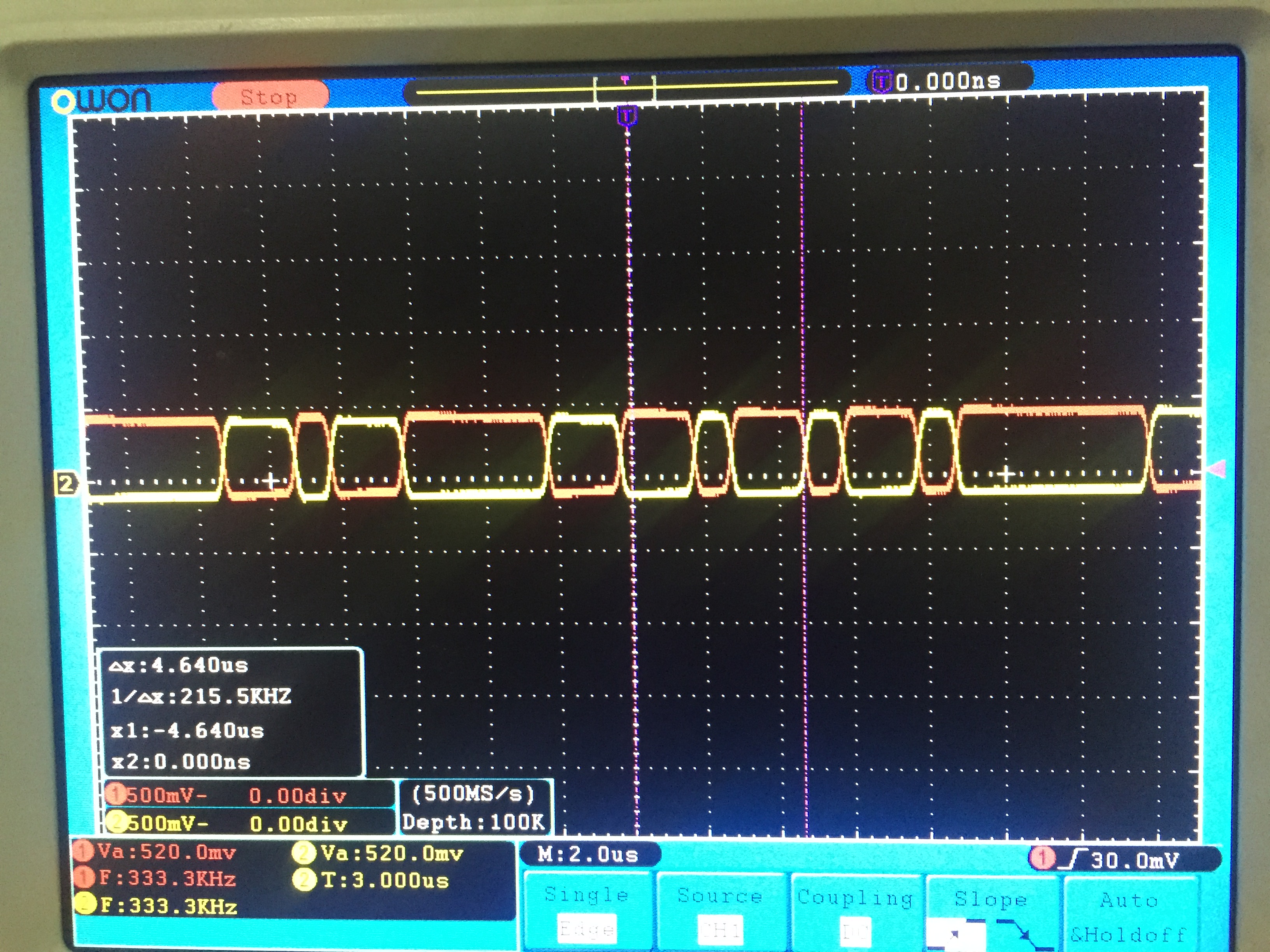
I have fed PRN sequence to IP and inverted PRN sequence(As we are interested in BPSK) to IQ.
QP and QN are left open.
I have tried varying DC offset to the PRN sequence, but no change in leakage.
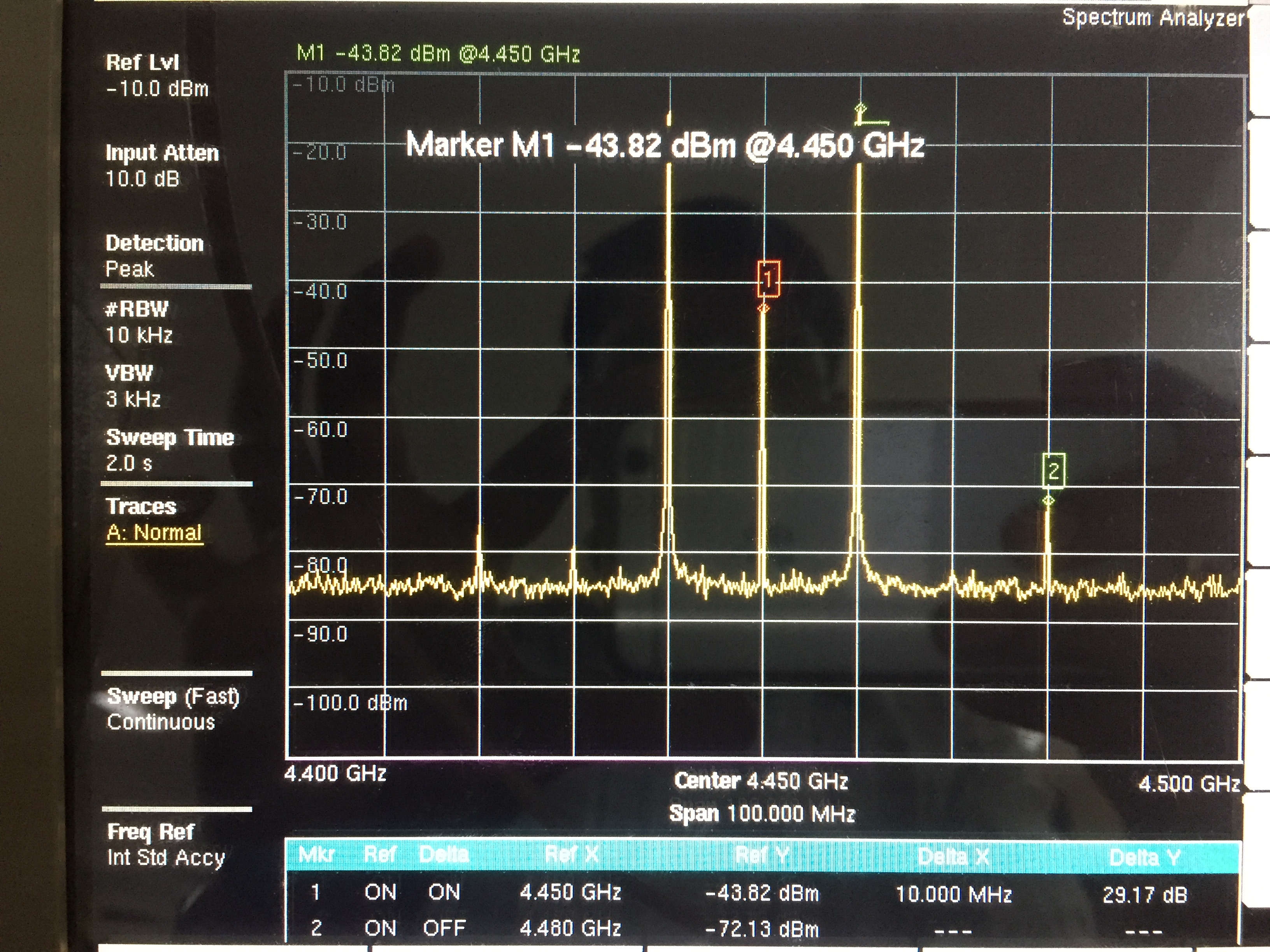
Following is the RFOUT
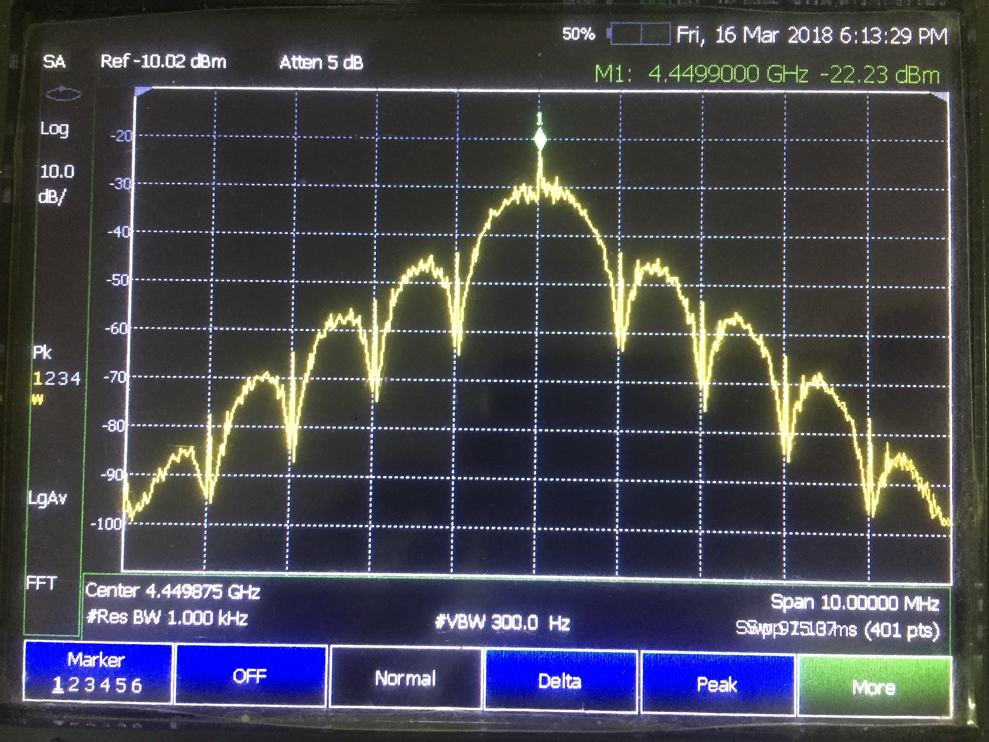
Observed that carrier leakage is prominent.
How to suppress these carrier leakage?
Our PRN sequence was
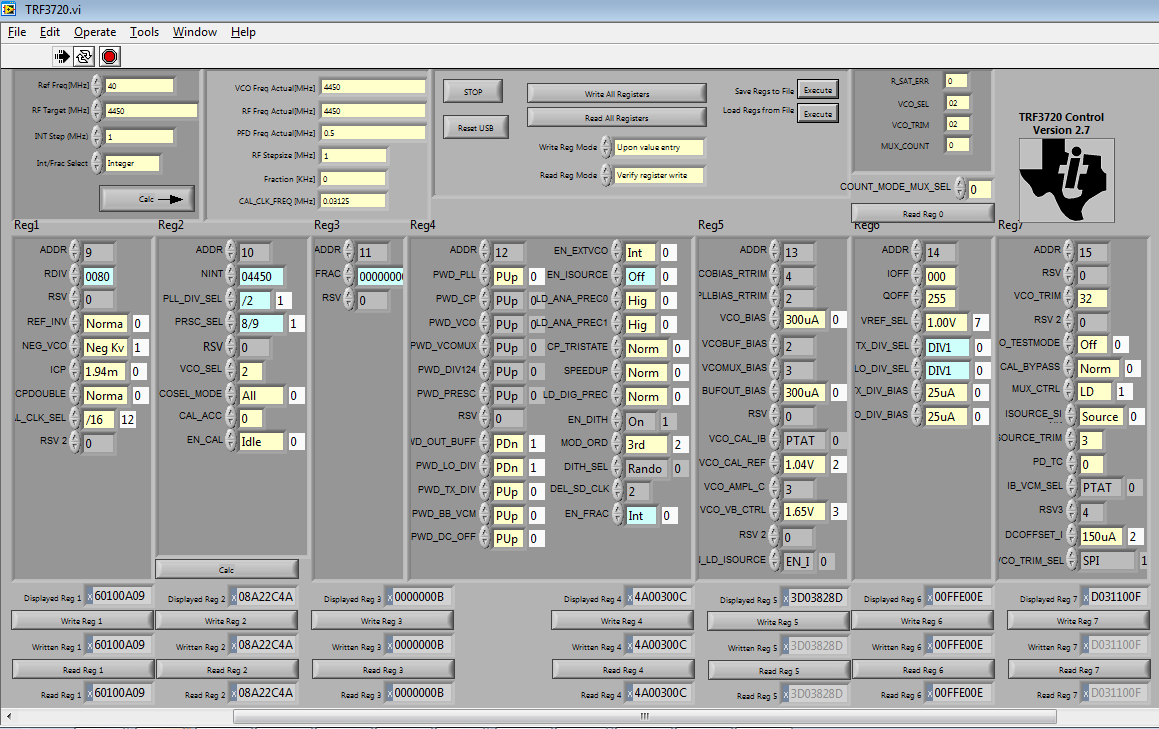
and GUI settings

Set Up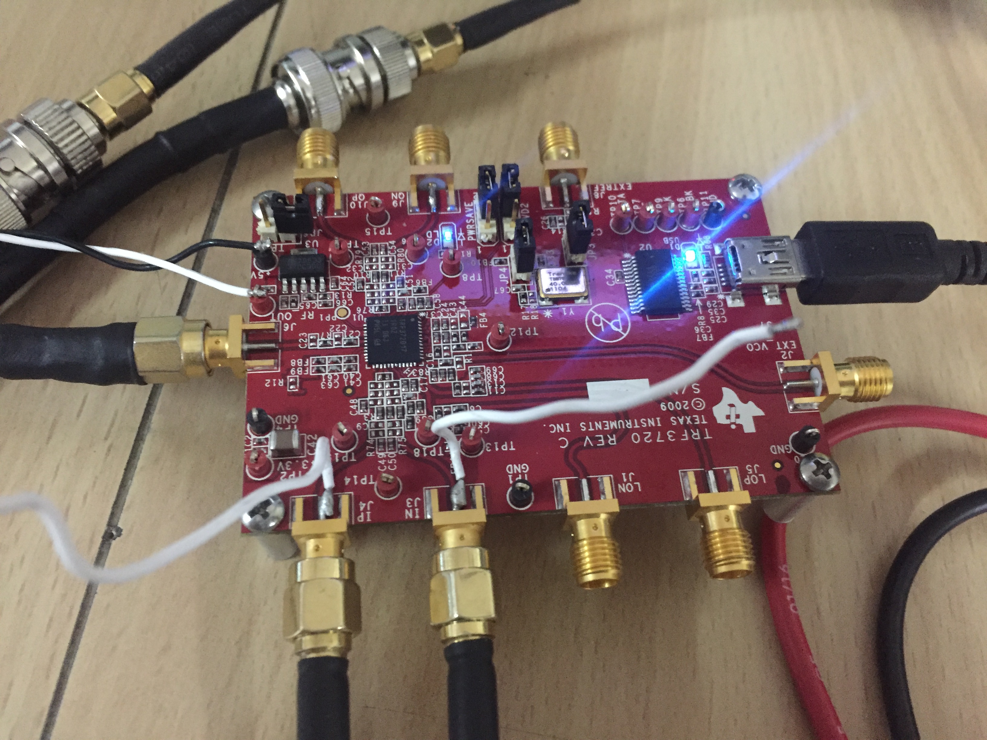
Please suggest in detail as i'm new to this IQ modulation concepts.
Observation: If PWD_BB_VCM=0 then 1.7V observed at R2,R3 and R10,R11 (IC side)
If PWD_BB_VCM=1 then 1.2V observed at R2,R3 and R10,R11 (IC side)
Is it acceptable? (I hope R2,R3 and R10,R11 are capacitors).
Thanks,
Raghu