This thread has been locked.

If you have a related question, please click the "Ask a related question" button in the top right corner. The newly created question will be automatically linked to this question.

IWR1443: IWR1443

Part Number: IWR1443
Other Parts Discussed in Thread: UNIFLASH, TIDEP-0091

I have a IWR1443 mounted on a PCB of my own design

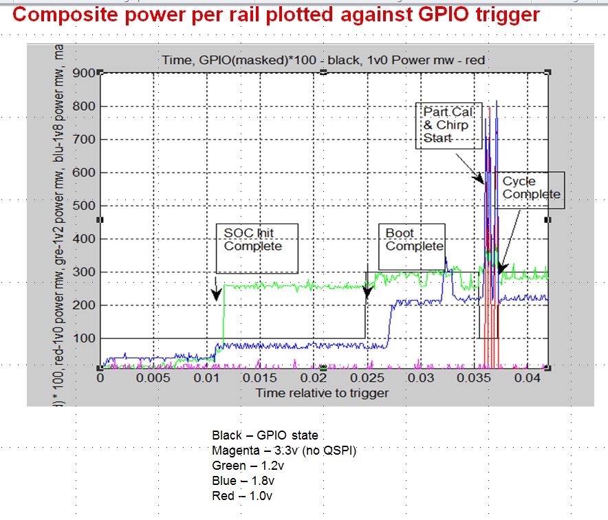
Can anyone tell me the current draw I should be seeing on each of the power rails fed to the device??

How does the voltage level on the NRESET pin effect these currents??

Am I correct in assuming that if the SOP pins are set to 1 0 1 when NRESET transition high I can flash my on board memory using the UNIFLASH program

directly communicating with RS232_RX (N5)  and RS232_TX(N6) of the IWR1443

Are there any other control signals that need to be set or sequenced for this to happen ? 

  Thanks

  • Hello,

    Hope you have already looked at the following document for design checks and bring up list.

    IWR1443 Checklist for Schematic Review, Layout Review, Bringup/Wakeup

    Rail specific current : 

    This is not published as you may check the lumped power/current graph provided in  Design Guide for :Power Optimization for IWR1443 77GHz-Level Transmitter Reference Design

    Have you had a change to take a look at the power sequence  mentioned in:

    5.9.1 Power Supply Sequencing and Reset Timing section in    IWR1443 Single-Chip 76- to 81-GHz mmWave Sensor datasheet

    This should provide the correct sequence for power up and expected reset  pin timing.

    SOP  pin information is provided in : Your assumption for mode selection is right, these pins  should be set and power up performed before reset release.

    IWR1443 Evaluation Module (IWR1443BOOST) mmWave Sensing Solution User's Guide

    IWR16xx/14xx Industrial Radar Family Technical Reference Manual

    Hope this helps you proceed. Please let us know if you have more questions we will have Hardware expert help you further.

    Thank you,

    Vaibhav

  • Hello,

    If you are looking for the minimum IO signals to boot:

    SOP[2.1.0] as '1'0'1'.

    nERROR_IN, WARM_RESET, nERROR_OUT pulled up to VIOIN

    Control UART (UART_Tx, UART_Rx) connected with pullups to VIOIN

    unless JTAG pins are connected to an XDS emulator, TMS pulldown

    nRESET should go from .3v to VIOIN for releaseing reset

    measure VBGAP .9v, 1.4v_APLL 1.4v, 1.4v_SYNTH 1.4v

    measure DVM (10Mohm) CLKP .5v, CLKM .5v, then using low capacitance prove, measure 40Mhz 1vptp on CLKP then CLKM

    using 2 channels normal triggering nRESET 0->1, check WARM_RESET output should output '0' during SOC initialization the '1'.

    measure all rail voltages to 5% limit

    Different power supply configurations  and software can provide for different current draw.

    std EVM power supply,  Flashing mode,                  SOP[2.0 101], no XDS emulator - .21A @ 5v

    std EVM power supply, Flashing mode,                   SOP[2.0 101],      XDS emulator - .28A @ 5v

    std EVM power supply, 1443 High Accuracy Lab, SOP[2.0 101],     no XDS emulator - .25A @ 5v

    std EVM power supply, 1443 High Accuracy Lab, SOP[2.0 101],          XDS emulator - .32A @ 5v

    swra577 power supply,  Flashing mode,                  SOP[2.0 101], no XDS emulator - .15A @ 5v

    swra577 power supply, Flashing mode,                   SOP[2.0 101],      XDS emulator - .21A @ 5v

    swra577 power supply, TIDEP91 Low Power Code, SOP[2.0 001], no XDS emulator - .185A @ 5v

    swra577 power supply, TIDEP91 Low Power Code, SOP[2.0 001],      XDS emulator - .245A @ 5v

    Expected rail currents during startup, depend on the software use case, in general

    Initialization, <25ma 3.3v, 1.2v varies as more core logic is used 0 - 400ma, 1.8v < .4a until radar chirp starts, 1.3v < .2a until radar chirp starts

    run - < 25ma 3.3v, 1.2v 400-600ma, 1.8v during chirp up to .9A, 1.3v (depends on what RF ports are turned on) upto 1.8A

    Regards

    Joe Quintal

    P.S. I have included the oscilloscope example for new TIDEP Low Power code (with swra577 power supply).  

    blue - nRESET

    green - WARM_RESET

    pink - GPIO-0 (application specific)

    yellow - 5v current probe 200ma/div

  • Hello,
    If you assert nRESET (=0) the 5v current into the PMIC is >100ma lower.
    Regards,
    Joe Quintal
  • Hello,

    The EVM would need to be modified to monitor each power rail, I have one example for TIDEP-0091 new Level Sensing code, this will work

    for IWR1443 ES2 (with longer boot time), or IWr1443 ES3 (shorter boot time).  The graph is in mw, you can divide by the rail voltage for current.

    Note: this graph is the power supply monitored, the PMIC power is a DCDC converter, that is Forced PWM for 1.0 (1.3) and 1.8v and PFM mode for others, see LP87524 datasheet.

    1.2v  - green

    1.3v (this is 1.0v for my setup) see swra577 - red

    1.8v - blue

    3.3v - magenta

    time 0 is the 0->1 nRESET release.

    Please see graph attached.

    Regards,

    Joe Quintal

  • THANKS JOE

    Best answer I've ever had.   

    my board doesn't have a pull down on TMS  

    Is this critical?

  • Hello

    Having a pulldown on TMS, or a pulldown on TCK prevents the Tap Controller from thinking a stray event causes JTAG test mode.

    Some previous designs created a plug for the XDS110 probe, connector with the resistor.

    Its only a problem, if you can't boot the device. 

    Regards,

    Joe Quintal