This thread has been locked.

If you have a related question, please click the "Ask a related question" button in the top right corner. The newly created question will be automatically linked to this question.

FDC2212-Q1: Questionable Excitation Signal on Sense Port

Part Number: FDC2212-Q1
Other Parts Discussed in Thread: TMS570LS3137, FDC2212

Dear TI team,

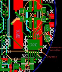
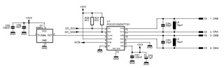
I am currently testing the FDC2212 on a self developed board with the TMS570LS3137 Hercules MCU. The circuit of the FDC2212 is shown in the picture below. For now the sensor is configured to only use one channel (Channel 0). The reference clock of 40MHz is divided by 2 by the setting of the corresponding register for Ch0. The Drive Current is set to be 

cap measurement circuit

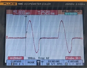
For testing the accuracy and feasibility for our application we have connected various capacities ranging from 10pF to 100pF. None of which we were able to measure correctly. So we captured the signal on port IN0A of the FDC which always looks like in the picture below with a peak voltage of about 0.6V.  Which, according to the snoa950.pdf document, is too low. It should be at least double of what we measured.

Also the signal shape looks completly different of what can be found in the forum provided by other users.

Can you provide any guidance of where the problem could be located? Whether we have a wrong setup of the sensor or a problem in the hardware?

Many thanks in advance!

  • Hi Stefan,

    Thank you for posting to the Sensing forum.

    You are correct that the sensor oscillation amplitude should be between 1.2 V and 1.8 V. The CHx_IDRIVE fields of the current drive control registers should be programmed so that the sensor oscillates between this specified voltage range. What is the current setting of these registers?

    I would recommend changing the sensor drive current to see if the increase in oscillation amplitude improves the behavior of the signal.

    Best regards,
    Nicole

  • Hello Nicole,

    thank you for your fast reply.

    And thank you for the tip with the CHx_IDRIVE field. I somehow missed this setting. The range of the voltage is now in a good range for our desired capacity values (between 1.3 and 1.65V). 

    Nonetheless I still believe there is a problem regarding the capacity conversion. The capacity can be converted using the equations (7) and (9). With this implemented I connected a 10pF capacitor to the FDC which resulted in a value of 347.682 pF (without subtraction of parasitc effects) and a 56pF cap wich resulted in 467.531pF. The difference of these two caps is much greater than the 46pF that I would expect. Any clue why this is the case? 

    Best regards,

    Stefan

  • Hi Stefan,

    If possible, can you attach a schematic and layout of your system? You can send these over private message if that is preferable. 

    Best regards,

    Nicole

  • Hi Nicole, 
    I can send you a private message with the full schematic and also the full layout. I already posted the schematic regarding the capacity conversion in my initial post. 

    Here you can see part of the current layout, zoomed in on the FDC and surroundings. It should be noted that the PCB has 6 layers. Green is the top layer (layer 2) and red the bottom layer (layer 6). Layer 2 is a GND plane, layer 3 +3.3V, layer 4 +1.2V and layer 5 contains some routings.


    I can send you the more detailed version in private if needed.

    Kind regards

    Stefan

  • Stefan,

    Nicole is out of office at the moment. I will reach out so we can private message on the detailed information.

    Regards,
    John