Other Parts Discussed in Thread: TDC7201
Dear TI team,
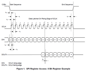
the datasheets for the TDC7200 (Fig. 1, page 8) and TDC7201 (Fig. 1, page 7) postulates:
DIN: SCLK rising edge
DOUT: SCLK falling edge
In consequence, the SPI-mode of a MCU SPI-block would have to be changed during a single register read transfer after sending the address
The 7200 diagram shows a real shift of DIN and DOUT in Fig. 1, but the diagram of Fig.21, page 22 does not!
The 7201 diagram does not show a shift.
What is the truth ? Which SPI mode(s) can we use?
Kind Regards
Martin
TDC7200:
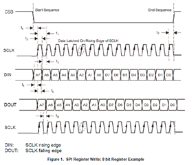
TDC7201: