This thread has been locked.

If you have a related question, please click the "Ask a related question" button in the top right corner. The newly created question will be automatically linked to this question.

DRV411: How to set the gain and compensation frequency externally?

Part Number: DRV411
Other Parts Discussed in Thread: TIPD184,

Hi,

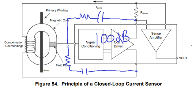
I have set up a current measurement circuit based on TIPD184. It seems to work fine.

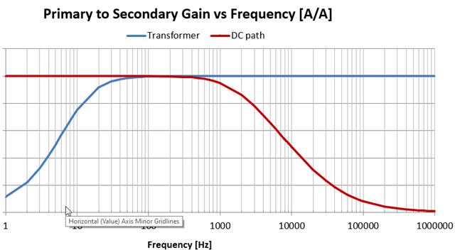
However now I would like to modifiy the compensation circuit to check how steady-state accuracy and bandwidth are affected.

Furthermore I would also like to check the measurement result when switching of the current spinning property.

In the datasheet of the DRV411 it is mentioned that Gain and Compensation Frequency can be set by selecting RF1, CF1 and RF2, CF2.

However since the resistor and capacitor are connected in series according to Fig. 57 of the datasheet, I am unaware of how the gain and compensation frequency can be calculated according to RF1, CF1, RF2 and CF2.

As a first step, I am thinking of getting the same gains which can be set by adjusting GSEL1 and GSEL2, while switching off the Spinning property.

Could you give me some guidance on my plan or refer any helpful documents?

Thanks a lot!

  • Hello Darshan,

    I just revisited this datasheet and reread the External Gain and compensation section.  The way I get it is that the gain is not compensation and is flat at about 100dB open loop gain.  You will need to model the gain of the core and the gain of your sensor.  The bandwidth will be limited by your core and transformer effect as there is a cross over the feedback of the DRV411(closed loop compensation) response and the response of the transformer effect form your core.  The Sense Amplifier as a 2MHz bandwidth.

  • Hi Javier,

    thanks for your response.

    Please allow me some further questions:

    1) So would you encourage me to model the Signal Conditioning Circuit + Coil Driver as an OpAmp with higher current driving capability (similiar to TIPD184 I've implemented an additional driver stage which will allow bipolar output voltages)  and an open loop gain of 100 dB?

    This would allow me to choose suitable R and C after simulating in TINA TI first. For Low-pass filters I am somehow more familiar with R & C being placed in parallel though.

    2) You mentioned that the core will be limiting the bandwidth of the sensor due to the transformer effect taking over at higher frequencies.

    However according to the datasheet the gain and compensation frequency are set by the signals applied to GSEL1 and GSEL2. The values 250 V/V and 1000 V/V and 3.8 kHz and 7.2 kHz are given in the datasheet irrespective of the core.

    Do these gains and frequency refer to the resistor/capacitor values which are connected internally in the IC in the way you have drawn above?

    I would like to choose R and C in a way that similar gains and f_zero can be achieved but the spinning circuit switched off.

    Thanks for your help. 


  • Darshan,

    1)You could do this and include the internal open loop gain of 100dB.

    2)The compensation is for the lower frequencies where the DRV411 drives the lower bandwidth and the current transformer effect takes over at larger frequency.  When driving with another driver will limit this explained below.  The gains and frequency of these do represent the internal feedback in the IC that represents the GSEL1 and GSEL2.  Based on the inductance of the compensation windings and Rshunt+compensation resistance to determine the pole created.  The datasheet recommendation is assuming that the dominate factor is the inductance.

    See following sections in datasheet: GAIN SELECTION AND COMPENSATION FREQUENCY

    I would encourage you use the spinning currents as this improves the offset and other issues with the hall sensor which will be some of the accuracy issue you will have.  The only issue is that the cross over form the DC path (where the DRV411 is driving the compensation coil) and the transformer path where the normally generated current transformer is made from the Primary to the Compensation windings. 

    The lower frequency is covered up to the DRV411 at limited by the gain and frequency you mentioned.  The transformer will take over at higher frequencies.  An image below is shown to illustrate this.  The issue I see is the at there is no low impedance path at higher frequency for the current transformer with a different driver.  Placing capacitors from the supplies to the compensation could deal with this to create the low impedance path at higher frequencies.

    From datasheet in Section:

    FUNCTIONAL PRINCIPLE OF CLOSED-LOOP CURRENT SENSORS WITH A HALL SENSOR