This thread has been locked.

If you have a related question, please click the "Ask a related question" button in the top right corner. The newly created question will be automatically linked to this question.

DRV5013-Q1: DRV5013-Q1 Detailed Layout Guidelines

Part Number: DRV5013-Q1

Hi,

I am Saran (PCB Design Engineer) from Eaton India Innovation Center LLP, India. We are working on a design which needs DRV5013-Q1 IC to be used for the application.

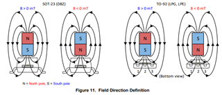
I'm looking at the DRV5013-Q1 chopper-stabilized Hall Effect Sensor's layout guidelines in detail. Apart from the standard datasheet layout guidelines we need more information regarding the component clearance of the other circuits from the Hall sensor position.

How much clearance/considerations is necessary to keep the rest of the circuits away from the hall sensor body. 

Kindly share the required information so as to follow the proper layout practice in our design to have good hall sensor performance.

  • Saran,

    Thanks for reaching out with your question.  The proximity of other devices would mainly depend on the current carried in nearby traces.  If there is an expectation that there could be a strong enough field to influence the sensor then it may be helpful to isolate the sensor.  In most cases, this is not a significant source of error, but if there are large transient currents then it could influence the device.

    The expected field can be calculated by: B = μ*I / (2*π*r) , where I is the current in the wire, and r is the distance from the wire.

    Thanks,

    Scott

  • Thanks Scott,

    Also should we consider avoiding copper beneath the sensor in all layers?(including any components on the other side of the PCB)

    Running coppers in the adjacent layers, will it degrade the sensor performance?

  • Saran,

    Since copper is not ferromagnetic, the DC magnetic field from a permanent magnet will permeate through the copper, so this should not be a significant issue unless there are large currents being carried adjacent to the sensor.  

    Apart from the copper traces, a sensors performance can be impacted if there are nearby ferromagnetic metals in the completed assembly.  These objects will channel the magnetic field which will distort the expected field behavior. If not carefully managed this can cause adverse effects.

    Thanks,

    Scott

  • Hi Scott,

    Thanks..! the information helps us in planning the layout task for us.

    It would be helpful if you could quantify on the specific clearance. For 3 Ampere current(AC or DC) what should be the specific clearance needs to be maintained from the sensor body. Could you be more specific on the actual clearance value for 3 Ampere current which would be appreciated.

    Thanks!!!

  • Saran,

    I did a quick calculation, and with 3A of current, if the sensor were 0.176 mm from the trace you would expect a possible field of 3.4 mT.  The distance from the sensing element would need to be at least 1 mm to ensure that the field from the wire is 0.6 mT or less. At a distance of 2.5mm, the field would be about 0.24 mT.

    Thanks,

    Scott

  • Scott,

    Thanks for the details. It really helped our layout process on the hall sensor part.

    I have one more question so that your comments will help me to overcome that criticality.

    Actually there is a connector that is being used in the design whose mounting pin comes close to the sensor IC(say 1mm is the clearance between them) and the material is nickel. What should be the minimum clearance to be followed between that nickel pin to the sensor body?

  • Saran,

    This is difficult to make estimations on as it will depend on the all of the geometries involved.  Nickel is one of the few ferromagentic metals, and as a result this pin will interact with the magnetic field produced by a permanent magnet.  The relative positions of the sensor, this connector pin, and the magnet will factor in for the actual field observed at the sensor.  If additionally this pin is carrying 3 A of current, then it will generate a field that wraps about the wire following the right hand rule, and this field will also interact with the magnetic field from the permanent magnet.

    The sensor is only sensitive to the field component which is directed orthogonal to the face of the sensor, so the relative orientation of the sensor can make a significant difference whether the field from the current in the connector or nearby traces is detected by the device.

    Also, any deflection or concentration of the magnetic field in the direction of sensitivity due to the nickel in the connector should be carefully considered.  If possible, I recommend that a prototype be built using as many of these factors as possible to verify functionality matches expectation.  In general,  however, maintaining some spacing from high current traces and limiting nearby ferromagnetic metals is a safe practice.

    Thank you,

    Scott

  • Thanks for your quick response...Scott...!!