This thread has been locked.

If you have a related question, please click the "Ask a related question" button in the top right corner. The newly created question will be automatically linked to this question.

DRV5053: DRV5053CAQDB

Part Number: DRV5053
Other Parts Discussed in Thread: DRV5055

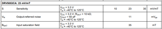
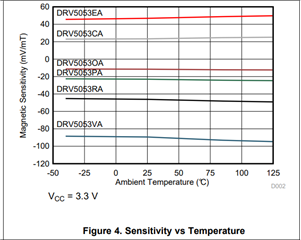
On the DRV5053CA hall effect device, it only specifies a nominal saturation flux of 35mT. Can TI comment on min and max saturation flux for this device? My measurements show this particular IC a saturation at ~68mT and I calculate the sensitivity of ~17mV/mT. I appreciate any input you can provide.  

  • Bill,

    Thanks for reaching out with your question.  The Sensitivity range for this device is shown here:

    These specifications at rated for the operating temperature range of the device, which for this device is -40C to 125C.  The typical temperature dependence of the sensitivity is shown in the following plot:

    The saturation output voltages for the device are shown here:

    Where +/- 35 mT input would be adequate to achieve either the minimum or maximum output value.  From the quiescent output voltage of 1 V, 35 mT input with a sensitivity of 23 mV/mT would produce an approximately 800 mV increase.  It is possible to calculate the expected worst case min/max range for BSAT using the Min and Max specifications for Sensitivity. At 10 mV/mT, an input of 80 mT would be required to reach the saturation output voltage of 1.8 V, and at 35 mV/mT, an input of 23mT would be needed.

    Your numbers of 68mT input with a sensitivity of 17mV/mT would suggest an increase in voltage of about 1.15 V from the quiescent value to reach saturation.  This would mean your quiescent output voltage is only 0.65V when no magnetic field is present.  If using a magnetometer to measure the field supplied to DRV5053, it is important to set the sensor location of the probe at the exact position of the sensing element in DRV5053.  Typically the sensitivity point for the probe is not the surface, but rather inset into the tip by some distance.  

    Thanks,

    Scott

  • Hello Scott: This answers most of the question THANKS! However, is it possible to get binned parts for sensitivity and saturation? I'm not use my system can tolerate the large sensitivity and saturation variation. 

  • Bill,

    Unfortunately, it is not possible with the existing assembly and test flows to produce binned parts with tighter tolerance of temperature drift performance.

    If you need to consider another device, you might look at DRV5055 which has much tighter Sensitivity ranges:

    This device is offered in multiple sensitivities. A# versions have the temperature compensation drift set to counterbalance against NdFeB type magnets which typically weaken by -0.12%/C.  The Z# versions have a flat temperature compensation implemented.

    This device is ratiometric, meaning that the output range will vary with Vcc.  As Vcc fluctuates, the output will remain at a constance %FS. When Vcc is used as the reference voltage in the sampling ADC, then this helps limit end measurement drift for Vcc.

    Thanks,

    Scott

  • Hello Scott: I wasn't interested in variation due to temperature. But the part you recommended with a tighter sensitivity range looks very promising. I think we can consider this thread to resolved. I begin a new thread if needed. THANKS a ton for you help and patience.