


Dear Experts,
could you please help to clarify Workaround #2 in Errata of AWR1843AOP for item PACKAGE#02A.
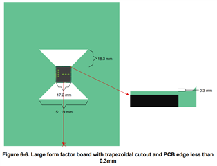
Below picture shows the workaround:
Is my understanding correct ?
- green color is the PCB
- white cutouts are going through the complete PCB, so basically having trapezoidal holes in the PCB
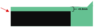
Is the 0.3mm marking placed incorrectly in above picture on the right ? Shouldn't it be from the device edge (black) to the edge of the PCB board ?
So something like this
Thanks and best regards,
Gregor

