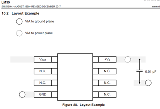
This is more of a general PCB layout question that is not limited to the LM35 - but I was noticing in the LM35 datasheet it suggests placing a power plane VIA between the bypass capacitor and the Vs+ pin. It's been my understanding that we always want to place the bypass capacitor as close as possible to the power pins, but placing the VIA between the pad and bypass capacitor suggests differently to me.
In general what is the best way to connect power pins to bypass capacitors when using a power plane?