This thread has been locked.

If you have a related question, please click the "Ask a related question" button in the top right corner. The newly created question will be automatically linked to this question.

AWR1843AOP: Question about RF LDO and PA LDO

Part Number: AWR1843AOP


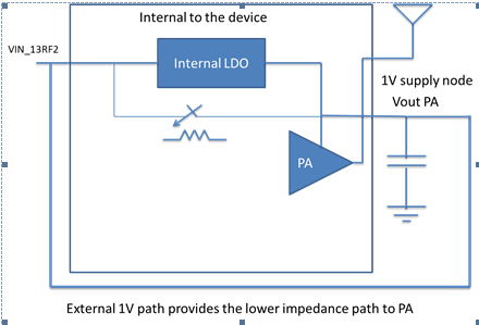
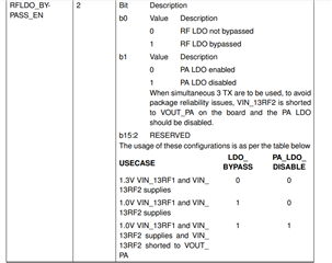
RF LDO and PA LDO are internal LDOs, but 'on/off' expressions are different as belows:  

RF LDO "non-bypassed/bypassed"

PA LDO "enabled/disabled"

I want to know the detail difference of RF LDO and PA LDO.

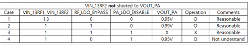
is it possible to share the detailed schematic including RF LDO and PA LDO ?

For example, the scheme with internal LDO is described as below links.

I want to know the detailed scheme including RF LDO and PA LDO. 

Thanks,

e2e.ti.com/.../3536882

  • Hello ,

    We might not be able to share the internal details, but here is the high level summary.

    1) For many of the internal RF circuits (LNA, LO etc.) we use 1V supply voltage. This could be either generated by feeding 1.3V from the external RF1/RF2 supply pins and using internal LDOs to generate 1V OR can be directly feed directly on the RF1/RF2 pins , in which case the internal LDOs are "bypassed". These LDOs dont have an external compensation cap- and hence the LDO o/p is not brought out on an external pin.

    2) For the TX PA specifically, we have a separate LDO called PA LDO. This LDO needs an external cap, hence is brought out on a pin. Incase you dont want to use this LDO , you can directly feed 1V supply at the LDO output pin and set the PA LDO to disable.

    regards,

    Vivek

  • The below snapshot from the Interface Control Document (ICD) might be helpful to understand the setting to use based on the voltages you are feeding.

  • by feeding 1.3V fr

    You mentioned that RF LDO and PA LDO are separated. RF LDO supplies 1V voltage to RF circuits and PA LDO supplies 1V voltage to PA only.


    In my radar application, I don't use 3-PAs simulatenously and I only use 1-PA at a time.

    So, I opened VIN_13RF2 and VOUT_PA to obtain effect of LDO PSRR and first USERCASE in ICD can be used.

    I checked VOUT_PA to see if the voltage was output properly (for all possible cases).

    Case 1,2,3 are resonable but case 4 are not understand.

    Although the PA LDO is disabled, the radar operates and VOUT_PA value is 0.95V.

    Can you give a point on this question?

    Of course, case 4 is not in the document.

    But I was curious becasuse it was different from the general LDO operation that I thought.

    Thanks

  • Hello Seunghoon,

    The image you had put in the above message is not visible. Are you referring to the Case 1/2/3 as the various combinations of the LDO Bypass and PA LDO disable settings? 

    regards,
    vivek

  • Hi Vivek,

    Yes. Case 1/2/3/4 are the various combinations of the LDO bypass an PA  LDO disable.

    You can see enlarged image if you click the figure.

  • I found the method of  increase of image size  now. 

  • Hello Seunghoon,

    The case 4 is not defined in the firmware , hence its behavior is undefined. That mode cannot be used.

    regards,
    vivek

  • Hi Vivek, 

    Ok. Thank you for reply.

    regards,

    Seunghoon