This thread has been locked.

If you have a related question, please click the "Ask a related question" button in the top right corner. The newly created question will be automatically linked to this question.

Regarding RTD circtuit(XTR112+RCV420+dcv010512dp)

Other Parts Discussed in Thread: XTR112, RCV420, DCP010512DB

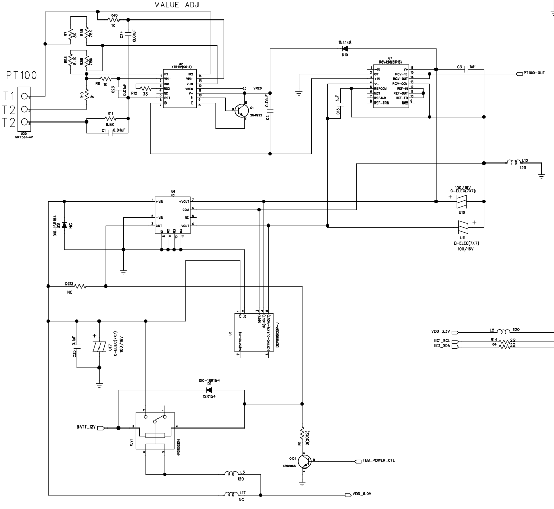
I am deveoping RTD temperature sensor with PT100/xtr112/rcv420/dcs010512dp.

It looks working well but there is very strange symptom which is DCS010512DP’s outputs are very strange one is +12V looking good but the other is -17V that should be around -12Voltage. If I remove RTD’s return wire, its voltages are changed from +12V to +17V and from -17V to -12V. I also wonder if this circuit and components are correct. Anybody help me.


  • Hi Yunsong,

    First, would you please attach the schematic as a .PDF or high-resolution image file?  The forum has limitations on image resolution and it's difficult to read the entire schematic.  So instead of clicking the "insert image" button, click the "insert file" button and upload it as a file. 

    Second, please confirm the part number of the isolated power-converter that you are using.  "DCS010512DP" is not a TI part number.  Are you using the DCP010512DB ?

    At first glance the XTR112 and RCV420 circuits appear to be connected properly.  What temperature range are you trying to relate to the 4-20mA output?

    Can you please clarify what you mean by the "RTD Return"?  Are you referring to pin 3 of the PT100 terminal block? I need to understand what you're removing from where to help diagnose this. 

    Please answer the questions and we'll get the worked out.

  • Hi ,

    First, I attached it as you mentioned with 'insert file', is it OK?

    Second, the part number is  DCV010512DP. sorry.

    temp range : -20-60 (but I want to change to -40~80)

    'RTD return' means pin 2 of PT100 terminal block component.

    Thank you for all your support.


  • Hi Yunsong,

    The file came through the same way, but no worries, I enlarged it and figured out what was connected. 

    First, please clarify which pin the "RTD return" connection is on your "PT100" terminal block.  There are two "T2" net names even though there are three terminals.  Is the "RTD Return" the top, middle, or bottom connection?  I'm currently assuming it's the bottom connection. 

    Second, I'm having trouble understanding the function of the L10 inductor that seems to connect the isolated common output of the DCV device to the input common connection.  This would seem to defeat the purpose of the isolation.  Are you sure that the secondary side of the DCV device is truly floating in relation to your system or Earth GND?


  • Hi Collin,

    I am sorry not to be accurate about it. I mean T2 is the middle pin.

    When I disconnected the middle wire, its voltage conditions were changed.


    Second, I want to isolate DCV's secondary output from system's main GND. Is there any faulty point?

  • Hi Yunsong,

    T2 (middle pin) is actually the negative input, while T2 (bottom pin) is where the return currents from the IR1 / IR2 reference current signals flows.  So the real effect of lifting the middle pin is that the negative input will go to the compliance voltage of the IR2 source and will be much higher than the positive input which should cause the output to go to 4mA.  I don't see how doing this would affect the power-supply voltages. 

    When you measure the power-supply voltages, what are you measuring between?  i.e. what electrical nets are the black and red probes connected to?

    I don't care for the inductor between the isolated and non-isolated GND potentials.  If you remove the inductor, does the issue go away?

    Does this issue in any way affect the operation of the circuit?