This thread has been locked.

If you have a related question, please click the "Ask a related question" button in the top right corner. The newly created question will be automatically linked to this question.

How to handle with the VCOM pin of the TDC1000-Q1?

Other Parts Discussed in Thread: TDC1000, LMV772, LMV881, OPA2357

Hi,

  There is a short description of the VCOM pin in the datasheet of TDC1000, "...note that the inputs of the LNA, PGA and comparators should be biased to the VCOM pin’s potential." I want to know to to do it exactly.

  I asked this question, because I encountered some problems. I failed to get any STOP pulse even if I set the ECHO_QUAL_THLD to 0h (-35mV), and saw the echo signal peak on the COMPIN reached far blew the threshold (Vpp > 500mV).

  • Cheng,

    Like any single supply opamp its output needs to swing around "analog common". In most cases that is VDD/2. Which is the same case for the TDC1000. If you follow the EVM schematic that should show you how to do it.

    More importantly DO NOT PROBE COMPIN pin directly unless unless you have a low capacitance/high impedance FET probe. (Tek6204 etc.). Any probe other than the type mentioned will add a DC offset to the signal going into COMPIN pulling it away from VCOM and thus STOP pulses cannot be generated. This is why if you look athe EVM schematic the COMPIN signal is buffered for the user to monitor it during debug.

    regards,

  • Please see the attached diagram showing  VCOM biasing internally as well as externally. VCOM is used to center the signal at VDD/2 to prevent clipping the lower cycles of the signal. If the path is AC coupled, then you would need to center the signal at the next amp stage by shifting the level by VCOM (if not biased internally). That is why in the diagram  the path is biased to VCOM prior to the COMIN pin.

    Receiver-path-VCOM-biasing.pdf

  • Thanks for you diagram!
    I had made a mistake in my circuit design, I didn't bias the COMPIN to VCOM through a resister. Now I had refine the design and get better result. However, I was still confused with the VCOM output and getting stucked . It was not a stable voltage signal (Should it stay on Vdd/2 stablly ?). Every time when TOF procedure begins, the VCOM will rise suddenly. This leads to a large unexpected signal input to following amplifiers, and finally cause false alarms. What's wrong?
  • If you can share your schematic and a scope picture showing the specifics of the signals in question I can better help you.
    Thanks,
  • My project is targeting proximity sensing. The pulse frequence of the TX/RX was 40KHz. The CLKIN is 2.56MHz.

    The above is the TDC1000Q1 partion of my circuit. Due to some reason, the inside LNA was bypassed. As a complementary, I placed a LMV772 between the LNAOUT and PGAIN to bring in extra 31dB gain.

    In addition, the reason for bypassing the inside LNA was the unexpected behavior of it. If the LNA was incorperated, the echo signal would become very bad.

    When I probed the RX PIN during TOF procedures, I could even see large signals outputing. It seemed that the LNA was outputing signal to RX side!? Very confusing.

    Are there any mistakes in my design? I will try post some screenshots of my oscilloscope later if I can.

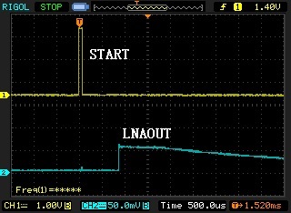
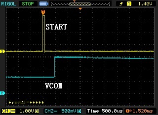
  • The above pictures are two screenshots from my oscilloscope. As you can see, the LNAOUT shew a rise edge when the echo listening began just after a power blanking period, so did the VCOM pin. (The internal LAN has been bypassed.)

    Is this normal or is there anything wrong?

    Regards.

  • Cheng,

    Below are my comments about your approach.

    1. Due to large attenuation of ultrasonic signal in the air it may be needed to drive the transducer with higher voltage. TDC1000 operating range is 2.7 to 5.5V and you may want to connect the VDD to a 5V supply instead to drive the transducer with higher energy (5 volt TX pulses).

    2. If the input single range of the PGA is approximately  700 mV or over, it would cause slewing condition, that is probably why the signal envelop you observed had an odd shape. I would bypass the PGA instead of the LNA as shown in the attached apps note (TDC1000-SNAA284). Although your application is proximately, the section including the  information about the design of external gain/filter and driving the transducer differentially would be applicable.

    3. The LMV772 may not be a good choice for this application for several reasons; a) the slew rate of 1.4 V/us (typ) is close to the margin particularly if you use VDD = 5V,  b) the offset is relatively high but ok if you use AC coupling in the path, c) The  input referred noise (en)  is relatively high, and d) if your application is battery powered, you would need an opamp with a shut-down pin.

    4. For the reasons above I suggest using the LMV881 or OPA2357 instead. Please see the attached apps notes for more information. You may use the LMV881 instead of the OPA2357 as shown in the second attached apps note (TDC1000-SNAA287).TDC1000_SNAA287.pdf


    2022.TDC1000_SNAA284.pdf


  • Yes what you are observing is normal. If the internal VCOM generator source  is selected via register settings, the VCOM source would be turned on/off automatically by the state machine to save power consumption in the battery operated applications.

    You can disable the internal VCOM feature and use an external source of VCOM continuously if needed. What you see in the scope screen is normal. The VCOM is turned on when the state machine turns the receiver path on. The VCOM ramps up and then when  the receiver is turned off by the state machine after the last STOP pulse (or after  the timer "TIMEOUT" time out), the external  0.01 uf  VCOM cap starts discharging, mainly through the scope probe if an active probe is not used.