Other Parts Discussed in Thread: TDC1000,
Hello,
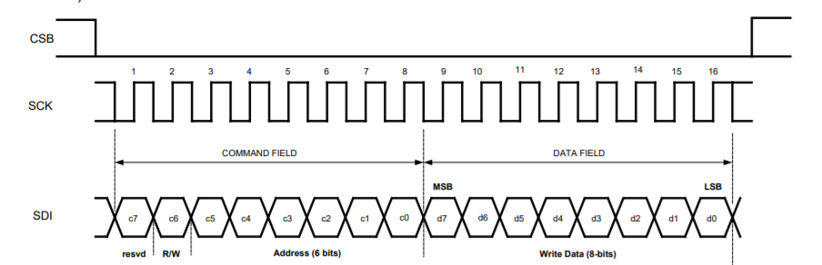
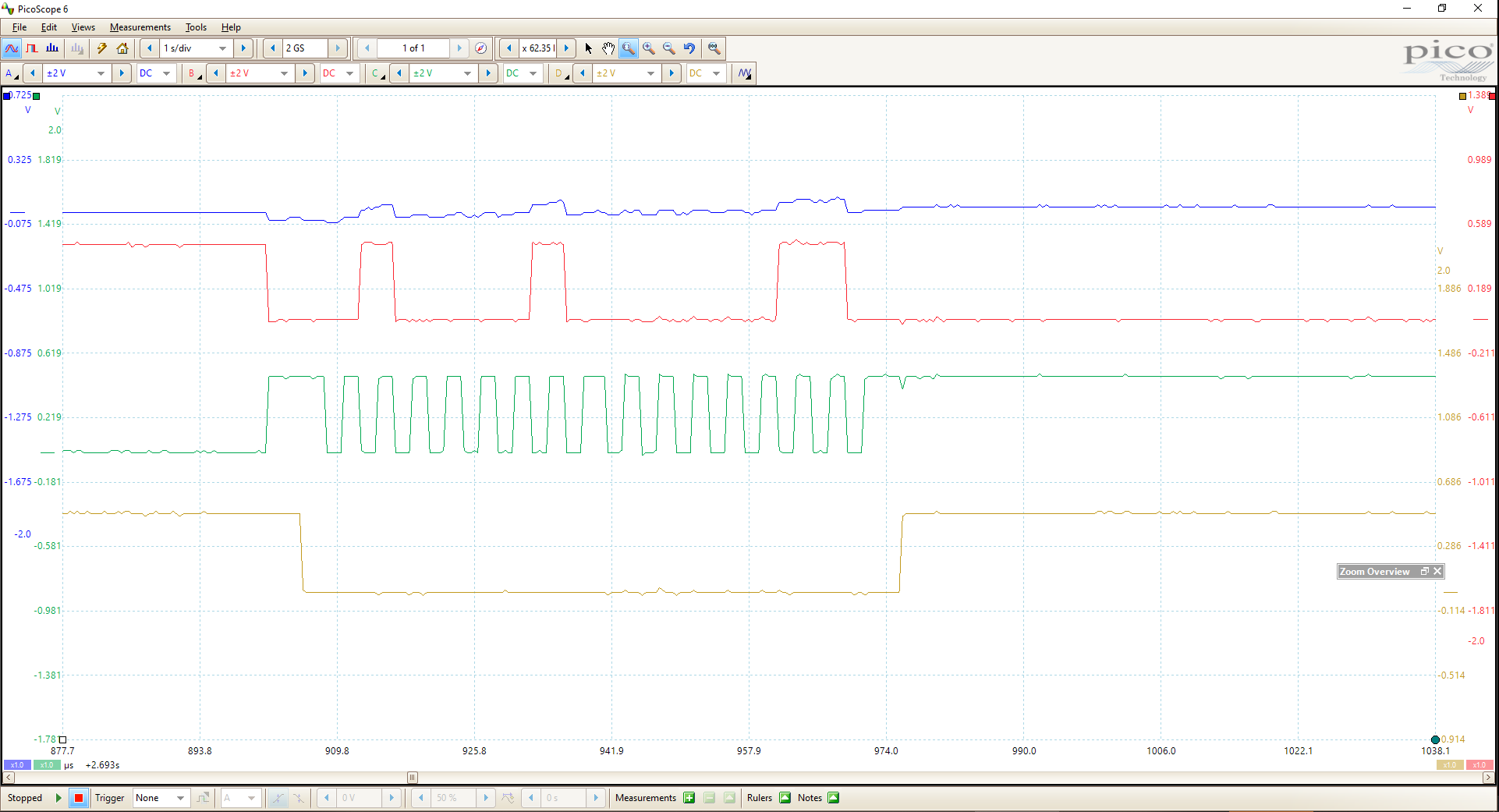
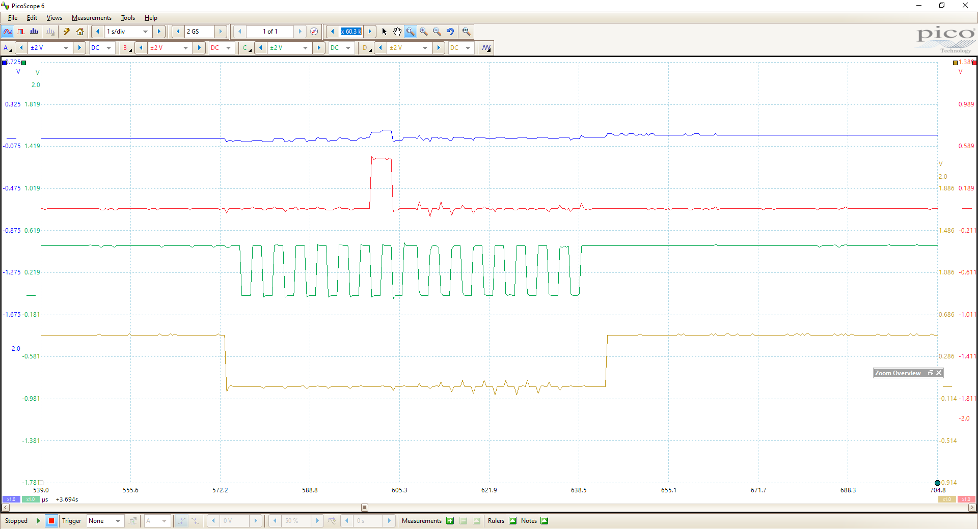
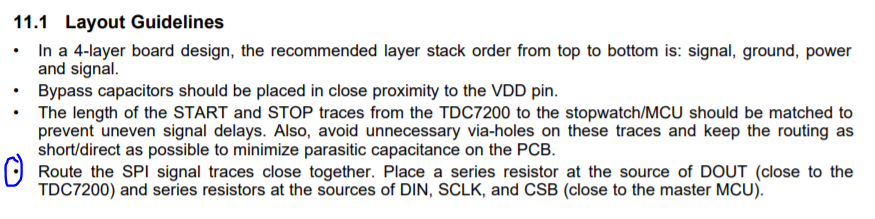
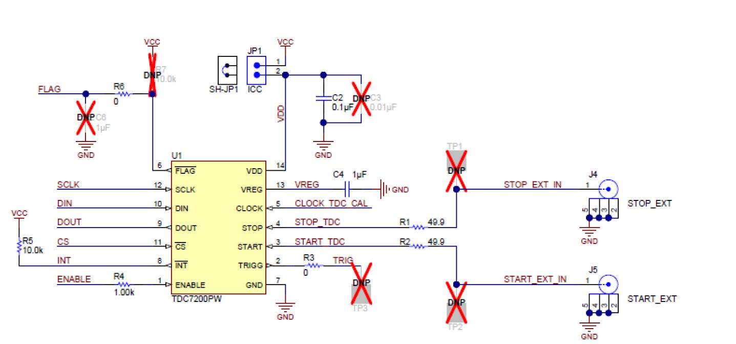
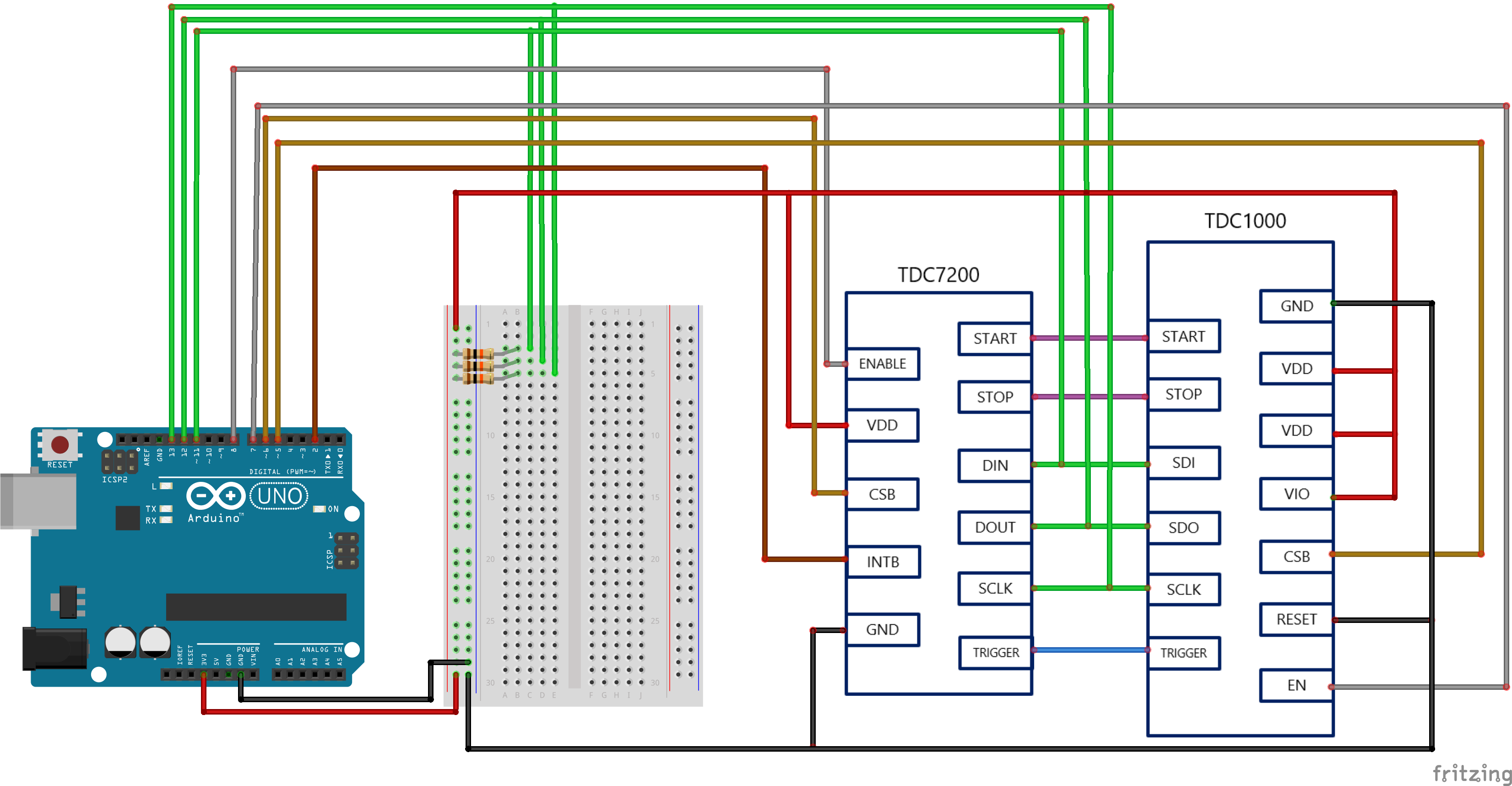
I am currently facing some troubles regarding the reading/writing to my TDC7200 with my Arduino Uno. I have tried circuits below with and without pullup resistors, and included the code I used below. For both circuits, I am able to read/write to my TDC1000 just fine, but for some reason I am unable to do the same for the TDC7200. Are the SPI conventions different between these two ICs?
Do let me know if I can provide for information that would provide more insight. Thank you for your time and attention.
Regards,
Jack
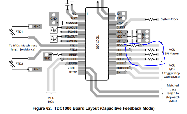
Connections:

#include <SPI.h>
#include <stdint.h>
int dt = 200;
float CLK_FREQ = 8*pow(10,6);//CLOCK frequency (default 8MHz)
float CLK_PERIOD = 1/CLK_FREQ;
uint32_t SPIfrequency = 20000000;
//*******************************TDC7200 REGISTER ADDRESS LIST*****************************
byte CONFIG1 = 0x00;
byte CONFIG2 = 0x01;
byte INT_STATUS =0x02;
byte INT_MASK = 0x03;
byte COARSE_CNTR_OVF_H = 0x04;
byte COARSE_CNTR_OVF_L = 0x05;
byte CLOCK_CNTR_OVF_H = 0x06;
byte CLOCK_CNTR_OVF_L = 0x07;
byte CLOCK_CNTR_STOP_MASK_H = 0x08;
byte CLOCK_CNTR_STOP_MASK_L = 0x09;
byte TIME1 = 0x10;
byte CLOCK_COUNT1 = 0x11;
byte TIME2 = 0x12;
byte CALIBRATION1 = 0x1B;
byte CALIBRATION2 = 0x1C;
//***************************END OF TDC7200 REGISTER ADDRESS LIST**************************
int selectTDC1000 = 5;
int selectTDC7200 = 6;
int enableTDC1000 = 7;
int enableTDC7200 = 8;
int dataReadyPin = 4;
int channelSelect = 3;
int INTBTDC7200 = 2;
int TDC7200clock = 9;
void setup() {
Serial.begin(9600);
Serial.println("----------------------Program Start-------------------------");
SPI.begin();
pinMode(TDC7200clock,OUTPUT);
pinMode(selectTDC1000, OUTPUT);
pinMode(selectTDC7200, OUTPUT);
pinMode(enableTDC1000, OUTPUT);
pinMode(enableTDC7200, OUTPUT);
pinMode(dataReadyPin, INPUT); //Unused in loops
pinMode(channelSelect, OUTPUT); //Unused in loops
analogWrite(TDC7200clock, 128);
digitalWrite(selectTDC1000, HIGH);
digitalWrite(selectTDC7200, HIGH); //Select is Active low, set to high @ initialise
digitalWrite(enableTDC1000, LOW);
digitalWrite(enableTDC7200, LOW); //Enable is Active high, set to low @ initialise
digitalWrite(enableTDC1000, HIGH);
digitalWrite(enableTDC7200, HIGH);
delay(dt);
TDC7200Write(CONFIG1,0x02);
TDC7200Write(CONFIG2,0x80);
TDC7200Write(INT_STATUS,0x06);
TDC7200Write(INT_MASK,0x89);
uint16_t readCONFIG1 = TDC7200Read(CONFIG1);
uint16_t readCONFIG2 = TDC7200Read(CONFIG2);
uint16_t readINT_STATUS = TDC7200Read(INT_STATUS);
uint16_t readINT_MASK = TDC7200Read(INT_MASK);
Serial.print("CONFIG1= ");
Serial.println(readCONFIG1,BIN);
Serial.print("\n");
Serial.print("CONFIG2= ");
Serial.println(readCONFIG2,BIN);
Serial.print("\n");
Serial.print("INT_STATUS= ");
Serial.println(readINT_STATUS,BIN);
Serial.print("\n");
Serial.print("INT_MASK= ");
Serial.println(readINT_MASK,BIN);
Serial.print("\n");
}
void loop() {
// put your main code here, to run repeatedly:
SPI.beginTransaction(SPISettings(SPIfrequency,MSBFIRST,SPI_MODE3));
delay(1000);
}
void TDC7200Write(byte address,byte data){
SPI.beginTransaction(SPISettings(SPIfrequency,MSBFIRST,SPI_MODE3));
digitalWrite(selectTDC7200, LOW);//between selectTDC1000 OR selectTDC7200
delayMicroseconds(100);
address |= 0x40;
SPI.transfer(address);
SPI.transfer(data);
digitalWrite(selectTDC7200, HIGH);
SPI.endTransaction();
};
byte TDC7200Read(byte address){
SPI.beginTransaction(SPISettings(SPIfrequency,MSBFIRST,SPI_MODE3));
digitalWrite(selectTDC7200, LOW);
delayMicroseconds(100);
//SPI.transfer(address);
SPI.transfer(address);
byte inByte = SPI.transfer(0x00);
digitalWrite(selectTDC7200, HIGH);
SPI.endTransaction();
return inByte;
};
EXAMPLE OUTPUT:
When R/W to TDC7200:
----------------------Program Start-------------------------
CONFIG1= 11111111
CONFIG2= 11111111
INT_STATUS= 11111111
INT_MASK= 11111111
When R/W to TDC1000:
----------------------Program Start-------------------------
CONFIG_0= 10
CONFIG_1= 10000000
CONFIG_2= 110
CONFIG_3= 1001