Other Parts Discussed in Thread: CC2640
Hello,
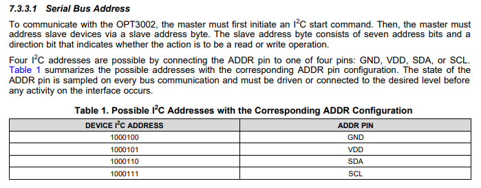
I'm using four OPT3002 on an I2C bus driven by CC2640r2. From the documentation I understand that there are four possible addresses. The Address line on the OPT3002 can be tied to VCC, GND, SDA, or SCL. I've configured each of the connectors so that they are wired correctly. I can plug two OPT3002 into any combination of mating connectors and they will work as expected - read data from the sensor. When I plug in a third OPT3002, the other two detectors continue to work as before, but the third detector doesn't work. If I remove one of the working detectors, the previously not working detector now works - again any two detectors will work. I've configured the CC2640r2 board file like so:
 Board_SPI0_CSN   | PIN_GPIO_OUTPUT_EN  | PIN_PULLUP      | PIN_GPIO_HIGH,                     /* CS pin at inactive level */
    Board_I2C0_SDA0  | PIN_INPUT_EN        | PIN_PULLUP      | PIN_OPENDRAIN,                     /* SDA pin pulled up*/
    Board_I2C0_SCL0  | PIN_INPUT_EN        | PIN_PULLUP      | PIN_OPENDRAIN,                     /* SCL pin pulled up*/
    Board_I2C0_INT   | PIN_INPUT_EN        | PIN_PULLUP      | PIN_IRQ_NEGEDGE,                   /* OPT3002 interrupt */
    Board_LOAD_CTRL  | PIN_GPIO_OUTPUT_EN  | PIN_PULLUP      | PIN_GPIO_HIGH   | PIN_OPENDRAIN,   /* Load control initially high */
    Board_UART_TX    | PIN_GPIO_OUTPUT_EN  | PIN_PULLUP      | PIN_GPIO_LOW,                      /* UART TX via debugger back channel */
    Board_UART_RX    | PIN_INPUT_EN        | PIN_PULLUP      | PIN_GPIO_LOW,                      /* UART RX via debugger back channel */
I understand that the I2C bus requires pull-ups. So, I'm using the internal facility on the CC2640r2 to pull up the bus lines. BTW, I've checked this performance against external 10K resistors and the performance is identical. I suspect that my PIN FUNC TABLE is incorrectly defined. Some pin here is not properly configured, causing the I2C bus to fail when I plug in a second device driving the SDA or SCL high with the pull up. assuming that the wiring is correct, which it must be, can anyone explain why I can't operate all four detectors on the I2C bus as advertised?
Any help is always appreciated.
Patrick