This thread has been locked.

If you have a related question, please click the "Ask a related question" button in the top right corner. The newly created question will be automatically linked to this question.

LDC2112: EMC Problems

Part Number: LDC2112

Hello TI team,

in the last days we got some troubles with our coil system at the emc tests.

We did get some fales press events in our button system. 

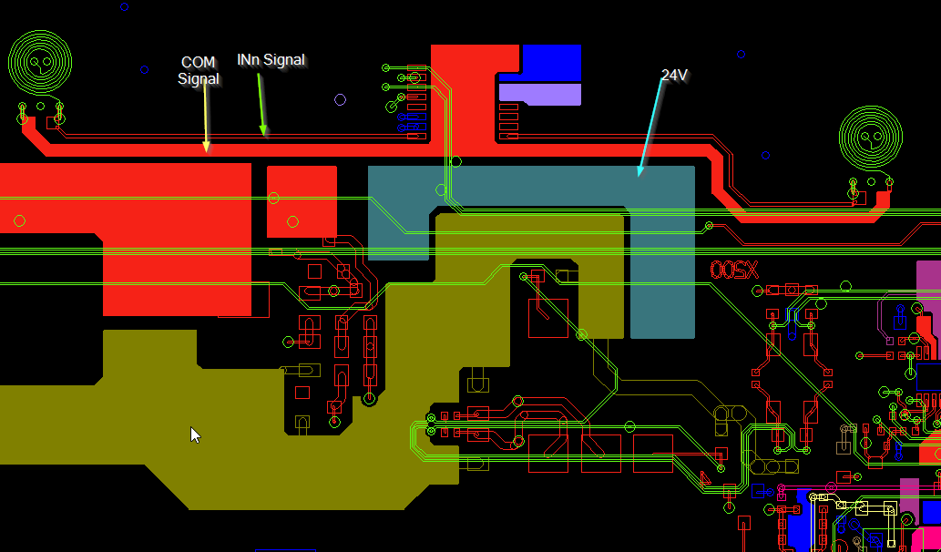
I suspect we have already found a mistake. This concers about the routing of the com and IN signals. I think we should root the signals like this example.

Because we are close to the supply voltage with our signals and the com and INn signals are rooted parallel.

Can you confirm it this way?

Furthermore I have a question to the coil shielding. 

Which signal should I use for the shielding?

Can I use the ground potential or should I am using the com signal?

Which would you prever?

Many thanks in advance.

Best regards,

Simon

  • Sorry, you will get the picture here.

    Picture 1:

    Picuture 2:

    Picture 3:

  • Hello Simon, 

    You are correct. Having a high voltage plane close to the COM signal can create additional parasitic capacitance between the two and it would be better to put a little more space between those two. 

    In regards to the shielding, use the COM plane shielding in your picture 2 for the LDC2112. The GND plane shielding is a general recommendation that applies to all devices but since the LDC211x contains the COM plane, it is recommended to use that for shielding instead. You can also have the COM plane surround the sensor coil but make sure there is a gap of at least 30% of the coil diameter around the coil. 

    Best Regards, 

  • Hello Justin,

    If we are going to use the COM to shield the sensor coil, so on which layers should we use the COM shielding?

    We are using a PCB with six layers and the sensor coil is on layer 1 till 4.

    Furthermore how wide should the area around the coil be?

    In addition, do you have any requirements for the routing width for the COM and INn signal?

    Thank you!

    Best regards

    Simon

  • Hello Simon, 

    We recommend using the layers above and below your INx trace to the sensor. 

    For around the coils, leave a gap that is 30% of your coil diameter around the coil. For example, if you have a 10mm coil, a 3mm gap around the outside of the coil should be applied. 

    We do not have any specific requirements on trace width but if you are shielding the INx trace with the multiple layers, then the COM should be at least twice the INx trace width. 

    Best Regards,

  • Hello Justin,

    I have one more question to the layout.

    Is it better to set vias at regular intervals for the COM line?

    Furthermore, do you have suggestions in which interval we have to set the vias?

    Or is it okay if we have two vias at the beginning and endig of the line?

    Thank you.

    Best regards

    Simon

  • Hello Simon, 

    When stitching the COM plane, treat it like a GND plane and take normal routing and EMI precautions when doing such. In general, an even spacing is a good idea and offsetting the second row to fill in gaps between the first will act as better shielding if that is what you need. 

    Best Regards,