Other Parts Discussed in Thread: ENERGIA, , TUSS4470
Hi,
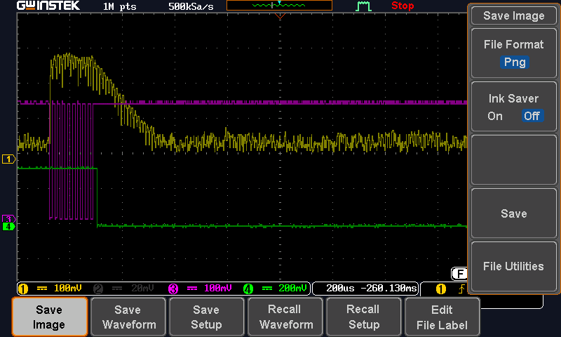
I'm writing a program in Code Composer Studio for the MSP430-F5529 to pulse the StemInc SMD15T21R111WL transducer at 1MHz for liquid level measurement and sample the result with the ADC12 module of the MSP430. The transducer is attached to a BOOSTXL-TUSS4470 and the pulse and sampling code is based on the Energia example for the BOOSTXL-TUSS4470. I ported the function burstBitBang from TUSS44x0_Ultrasonic.cpp, but the ported code does not start the sampling process soon enough to capture the entire envelope. I tested this transducer at 1MHz with the TUSS44x0 EVM GUI and the full envelope is displayed. My first coding attempt was to begin sampling immediately after the pulses are sent, but the TUSS4470 envelope from VOUT is halfway finished before the sampling process begins (see photo 1) Another attempt was to start the sampling process before pulses are sent to the transducer. This also does not begin quickly enough (photo 2). I also attempted to start conversion immediately after the pulses using a single register level command, ADC12SC to reduce the code overhead of Driver Library but this did not noticeably improve the sample start time. Are there any examples that demonstrate how the EVM GUI captures the full output envelope of a 1 MHz transducer? The code I wrote is included below. Thanks for any feedback or ideas,
John
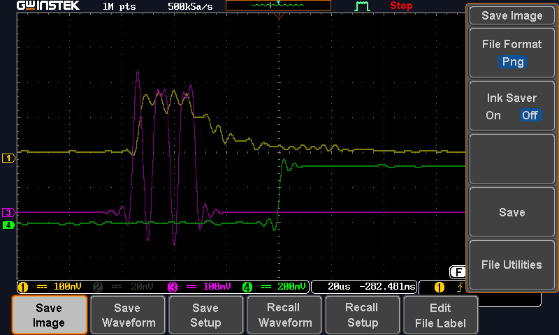
Photo 1: start conversion after bitBang
purple: pulses
yellow: VOUT envelope
green: sample start
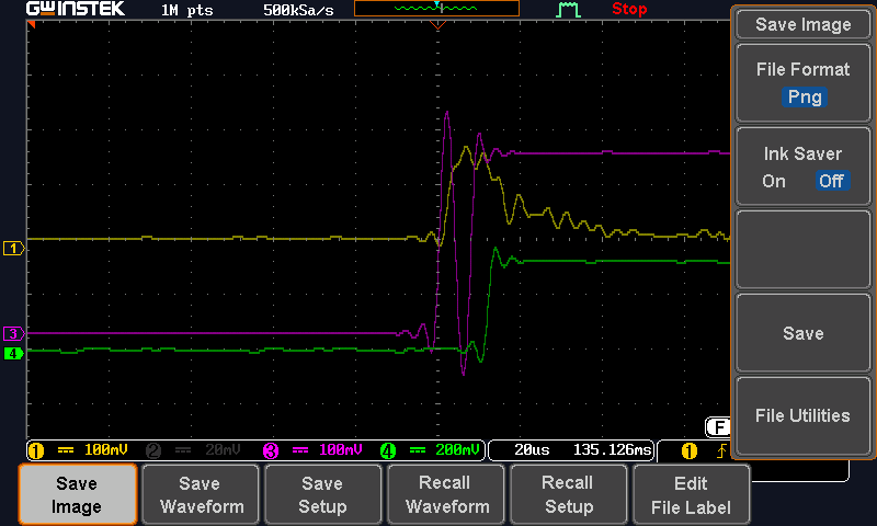
Photo 2 : start conversion before bitBang
// code sources:
// A : msp430_driverlib_2_91_13_01\examples\MSP430F5xx_6xx\usci_a_spi/usci_a_spi_ex1_master.c
// B : TUSS4470 examples\examples\VOUT_ADC_Processing\TUSS44x0_ultrasonic.cpp
// C : msp430_driverlib_2_91_13_01\examples\MSP430F5xx_6xx\adc12_a/adc12_a_ex5_repeatedSingle.c
// D : msp430_driverlib_2_91_13_01\examples\MSP430F5xx_6xx\usci_b_i2c\usci_b_i2c_ex3_slaveRxSingle.c
#include "driverlib.h"
#include <stdio.h>
// Prototypes
void initialize();
void initClocks();
void initTUSS4470();
void initSPI();
void initI2C();
void initADC12();
void writeRegTUSS4470 (uint8_t address, uint8_t value);
uint8_t * tuss44x0_regAddParity(uint8_t addr, uint8_t data);
uint8_t tuss44x0_parity(uint8_t * spi16Val);
uint8_t parity16(unsigned int ino);
unsigned int BitShiftCombine( unsigned char x_high, unsigned char x_low);
void executeTOFandSample();
void ADC12PreOps();
void ADC12PostOps();
void blinkLED();
void USCI_B0_ISR(void);
void ADC12ISR (void);
// SPI Variables
#define SPICLK 500000
uint8_t SPIInitReturnValue = 0;
uint8_t receiveData;
// Clock/UCS variables
uint16_t NMIstatus;
#define LF_CRYSTAL_FREQUENCY_IN_HZ 32768
#define HF_CRYSTAL_FREQUENCY_IN_HZ 4000000
#define MCLK_DESIRED_FREQUENCY 4000000 // 4 MHz
#define MCLK_FLLREF_RATIO MCLK_DESIRED_FREQUENCY / UCS_REFOCLK_FREQUENCY
uint32_t myACLK = 0;
uint32_t mySMCLK = 0;
uint32_t myMCLK = 0;
// TOF Variables
const uint8_t bitBangDelay = 0 ;
// ADC variables
#define ADC12_Num_of_Indexes 10
#define ADC12_Num_of_Results 125
volatile uint8_t ADC12_results_index1 = 0;
volatile uint8_t ADC12_results_index2 = 0;
int ADCValuesCounterIndex = 0;
int ADCValuesCounterResults = 0;
volatile uint16_t ADC12_results[ADC12_Num_of_Indexes][ADC12_Num_of_Results] = {};
void main(void)
{
int i = 0;
initialize();
// test loop
for (i = 0; i < 2000; i++) {
executeTOFandSample(); // TUSS4470 - excite transducer and sample output with MSP430 ADC12
__delay_cycles(10000000); // delay 2.5 seconds
}
__bis_SR_register(LPM0_bits + GIE);
__no_operation();
}
//// Initialization /////
void initialize() {
WDT_A_hold(WDT_A_BASE); //Stop watchdog timer
P1DIR |= 00000001; // prepare LED communication
__bis_SR_register(GIE); // enable interrupts
initClocks(); // initialize MSP430 clocks
initSPI(); // initialize SPI communication for MSP430 -> TUSS4470
initADC12(); // initialize ADC12 A/D converter in MSP430F5529
initTUSS4470(); // initialize/configure TUSS4470
}
void initClocks() {
UCS_setExternalClockSource(LF_CRYSTAL_FREQUENCY_IN_HZ, HF_CRYSTAL_FREQUENCY_IN_HZ);
// Setup ACLK to use REFO as its oscillator source
UCS_initClockSignal(UCS_ACLK, // Clock you're configuring
UCS_REFOCLK_SELECT, // Clock source
UCS_CLOCK_DIVIDER_1 // Divide down clock source by this much
);
// Set the FLL's clock reference clock source
UCS_initClockSignal(UCS_FLLREF, // Clock you're configuring
UCS_REFOCLK_SELECT, // Clock source
UCS_CLOCK_DIVIDER_1 // Divide down clock source by this much
);
// Configure the FLL's frequency and set MCLK & SMCLK to use the FLL as their source
UCS_initFLLSettle(MCLK_DESIRED_FREQUENCY, MCLK_FLLREF_RATIO); // MCLK frequency, Ratio between MCLK and FLL's reference clock source
myACLK = UCS_getACLK();
mySMCLK = UCS_getSMCLK();
myMCLK = UCS_getMCLK(); // verify 4MHZ master clock speed
}
//// ADC Initialization ////
// code source: C
void initADC12() {
GPIO_setAsOutputPin(GPIO_PORT_P8, GPIO_PIN2); // timing test
GPIO_setOutputLowOnPin(GPIO_PORT_P8,GPIO_PIN2); //Set P2.7 for slave reset
// ADC clock source is ADC12OSC -> default source is MODOSC @ 5MHZ
// SMCLK and MCLK = 4MHZ
// Calculate minimum required sample time
// calculation source: MSP430 User guide section 28.2.5.3 'Sample Timing Considerations'
// The resistance of the source RS and RI affect tsample. The following equation can be used to calculate the
// minimum sampling time tsample for a n-bit conversion, where n equals the bits of resolution:
// t.sample > (RS + RI) × ln(2n+1) × CI + 800 ns
// Substituting the values for RI and CI given above, the equation becomes:
// t.sample > (RS + 1.8 KOhm) × ln(2n+1) × 25 pF + 800 ns
// For example, for 12-bit resolution, if RS is 10 KOhm, t.sample must be greater than 3.46 µs.
// using 4.2 KOhms output resistance of TUSS4470
// sample > (4.2 Kohm + 1.8 KOhm) * ln(2 ^ (12 + 1)) * 25 + 800ns
// sample > 2.151 us
// minimum sample time = 2.15uS
// if ADC clock = 4MHZ, 1 cycle = 0.25 uS, a minimum of 9 cycles (2.25 uS) is required to meet minimum sample time of 2.15 us (16 cycles or 3.2 uS is closest driverlib option)
// configure REF (reference voltage) module
while(REF_ACTIVE == Ref_isRefGenBusy(REF_BASE));
Ref_setReferenceVoltage(REF_BASE, REF_VREF1_5V);
Ref_enableReferenceVoltage(REF_BASE);
__delay_cycles(100);
//Enable A/D channel A0
GPIO_setAsInputPin(GPIO_PORT_P6, GPIO_PIN5); // configure Pin 6.5 as input - connected to physical TUSS4470 pin 2 / a.k.a VOUT
// GPIO_setAsPeripheralModuleFunctionInputPin(GPIO_PORT_P6, GPIO_PIN5); // configure Pin 6.5 as input - connected to physical TUSS4470 pin 2 / a.k.a VOUT
// ADC12_A_init(ADC12_A_BASE, ADC12_A_SAMPLEHOLDSOURCE_SC, ADC12_A_CLOCKSOURCE_ADC12OSC, ADC12_A_CLOCKDIVIDER_1);
ADC12_A_init(ADC12_A_BASE, ADC12_A_SAMPLEHOLDSOURCE_SC, ADC12_A_CLOCKSOURCE_SMCLK, ADC12_A_CLOCKDIVIDER_1);
ADC12_A_setupSamplingTimer(ADC12_A_BASE, ADC12_A_CYCLEHOLD_16_CYCLES, ADC12_A_CYCLEHOLD_16_CYCLES, ADC12_A_MULTIPLESAMPLESENABLE); // sample time = 16 Cycles ~ 3.2 uS at 5MHZ ADC clock
ADC12_A_configureMemoryParam param = {0}; //Configure Memory Buffer
param.memoryBufferControlIndex = ADC12_A_MEMORY_0; // Base address of the ADC12_A Module
param.inputSourceSelect = ADC12_A_INPUT_A0; // Map input A0 to memory buffer 0
param.positiveRefVoltageSourceSelect = ADC12_A_VREFPOS_INT;
// param.positiveRefVoltageSourceSelect = ADC12_A_VREFPOS_AVCC; // Vref+ = AVcc
param.negativeRefVoltageSourceSelect = ADC12_A_VREFNEG_AVSS; // Vref- = AVss
param.endOfSequence = ADC12_A_NOTENDOFSEQUENCE; // Memory buffer 0 is not the end of a sequence
ADC12_A_configureMemory(ADC12_A_BASE ,¶m);
ADC12_A_enable(ADC12_A_BASE);
}
//// SPI Initialization ////
// code source: A
void initSPI() {
GPIO_setAsOutputPin(GPIO_PORT_P2, GPIO_PIN7); // CS
GPIO_setOutputHighOnPin(GPIO_PORT_P2,GPIO_PIN7); //Set P2.7 for slave reset
GPIO_setAsPeripheralModuleFunctionInputPin(GPIO_PORT_P3, GPIO_PIN0); // MOSI
GPIO_setAsPeripheralModuleFunctionInputPin(GPIO_PORT_P3, GPIO_PIN1); // MISO
GPIO_setAsPeripheralModuleFunctionInputPin(GPIO_PORT_P3, GPIO_PIN2); // CLK
//Initialize Master
USCI_B_SPI_initMasterParam param = {0};
param.selectClockSource = USCI_B_SPI_CLOCKSOURCE_SMCLK;
param.clockSourceFrequency = UCS_getSMCLK();
param.desiredSpiClock = SPICLK;
param.msbFirst = USCI_B_SPI_MSB_FIRST;
// TUSS4470 : use SPI_MODE1 CPOL=0, CPHA=1 - from Energia code example //
param.clockPhase = USCI_B_SPI_PHASE_DATA_CAPTURED_ONFIRST_CHANGED_ON_NEXT; // CPHA=1
param.clockPolarity = USCI_B_SPI_CLOCKPOLARITY_INACTIVITY_LOW; // CPOL=0
SPIInitReturnValue = USCI_B_SPI_initMaster(USCI_B0_BASE, ¶m);
if (STATUS_FAIL == SPIInitReturnValue){
return;
}
}
//// TUSS4470 Initialization ////
void initTUSS4470()
{
GPIO_setAsOutputPin(GPIO_PORT_P2, GPIO_PIN5); // configure MSP430 to output bitBang to Port 2, Pin 5 or TUSS4470 IO2 / pin 40
// recommended TUSS4470 register settings from INDUS_REG_USER_MEMSPACE_447-StemincTDCXDCR_Optimized.txt
// e2e.ti.com/.../927400
writeRegTUSS4470(0x10 ,0x5F); // (BPF_CONFIG_1)
writeRegTUSS4470(0x11 ,0x00); // (BPF_CONFIG_2)
writeRegTUSS4470(0x12 ,0x1C); // (DEV_CTRL_1)
writeRegTUSS4470(0x13 ,0xC1); // DEV_CTRL_2)
writeRegTUSS4470(0x14 ,0x00); // (DEV_CTRL_3)
writeRegTUSS4470(0x15 ,0x00); // (DEV_CTRL_4)
writeRegTUSS4470(0x16 ,0x40); // (VDRV_CTRL)
writeRegTUSS4470(0x17 ,0x07); // (ECHO_INT_CONFIG)
writeRegTUSS4470(0x18 ,0x14); // (ZC_CONFIG)
writeRegTUSS4470(0x19 ,0x00); // (XFMR_DRV_LIM)
writeRegTUSS4470(0x1A ,0x08); // (BURST_PULSE)
writeRegTUSS4470(0x1B ,0x02); // (TOF_CONFIG)
writeRegTUSS4470(0x1C ,0x08); // (DEV_STAT)
writeRegTUSS4470(0x1D ,0xB9); // (DEVICE_ID)
writeRegTUSS4470(0x1E ,0x02); // (REV_ID)
writeRegTUSS4470(0x1F ,0x00); // (DEV_TI_UNLOCK)
}
// code source: B
//// write register values to TUSS4470 over SPI bus ////
void writeRegTUSS4470 (uint8_t address, uint8_t value) {
uint8_t *regValPtr;
uint8_t tuss4470regWriteArray[2];
regValPtr = tuss44x0_regAddParity(address, value);
tuss4470regWriteArray[0] = *regValPtr;
tuss4470regWriteArray[1] = *(regValPtr + 1); // increment pointer 1 byte
//Enable SPI module
USCI_B_SPI_enable(USCI_B0_BASE);
//Wait for slave to initialize
__delay_cycles(100);
//USCI_B0 TX buffer ready?
while (!USCI_B_SPI_getInterruptStatus(USCI_B0_BASE, USCI_B_SPI_TRANSMIT_INTERRUPT)) ;
GPIO_setOutputLowOnPin (GPIO_PORT_P2,GPIO_PIN7); // set CS LOW to signal transfer ready to begin
USCI_A_SPI_transmitData(USCI_B0_BASE,tuss4470regWriteArray[0]);
while(USCI_B_SPI_isBusy(USCI_B0_BASE));
USCI_A_SPI_transmitData(USCI_B0_BASE,tuss4470regWriteArray[1]);
while(USCI_B_SPI_isBusy(USCI_B0_BASE));
GPIO_setOutputHighOnPin (GPIO_PORT_P2,GPIO_PIN7); // set CS HIGH to signal transfer & receive complete
}
// code source: B
//// Execute Time of Flight and Sample ////
void executeTOFandSample() {
// number of pulses : 12, bitBangDelay = n/a
ADC12PreOps(); // ADC12 configuration
__bis_SR_register(GIE); // disable interrupts
writeRegTUSS4470(0x1B, 0x00); // TOF_CONFIG's CMD_TRIGGER to 0
writeRegTUSS4470(0x1B, 0x01); // TOF_CONFIG's CMD_TRIGGER to 1 (enable burst mode)
// ADC12_A_startConversion(ADC12_A_BASE, ADC12_A_MEMORY_0, ADC12_A_REPEATED_SINGLECHANNEL);
P2OUT ^= 0x20; // send pulse to P2OUT -> TUSS4470 IO2 (PIN 40) // MSP430 PORT 2, PIN 5
// __delay_cycles(bitBangDelay);
P2OUT ^= 0x20;
// __delay_cycles(bitBangDelay);
P2OUT ^= 0x20;
// __delay_cycles(bitBangDelay);
P2OUT ^= 0x20;
// __delay_cycles(bitBangDelay);
P2OUT ^= 0x20;
// __delay_cycles(bitBangDelay);
P2OUT ^= 0x20;
// __delay_cycles(bitBangDelay);
P2OUT ^= 0x20;
// __delay_cycles(bitBangDelay);
P2OUT ^= 0x20;
// __delay_cycles(bitBangDelay);
P2OUT ^= 0x20;
// __delay_cycles(bitBangDelay);
P2OUT ^= 0x20;
// __delay_cycles(bitBangDelay);
P2OUT ^= 0x20;
// __delay_cycles(bitBangDelay);
P2OUT ^= 0x20;
// __delay_cycles(bitBangDelay);
P2OUT ^= 0x20;
// __delay_cycles(bitBangDelay);
P2OUT ^= 0x20;
// __delay_cycles(bitBangDelay);
P2OUT ^= 0x20;
// __delay_cycles(bitBangDelay);
P2OUT ^= 0x20;
// __delay_cycles(bitBangDelay);
P2OUT ^= 0x20;
// __delay_cycles(bitBangDelay);
P2OUT ^= 0x20;
// __delay_cycles(bitBangDelay);
P2OUT ^= 0x20;
// __delay_cycles(bitBangDelay);
P2OUT ^= 0x20;
// __delay_cycles(bitBangDelay);
P2OUT ^= 0x20;
// __delay_cycles(bitBangDelay);
P2OUT ^= 0x20;
// __delay_cycles(bitBangDelay);
P2OUT ^= 0x20;
// __delay_cycles(bitBangDelay);
P2OUT ^= 0x20;
// __delay_cycles(bitBangDelay);
__bis_SR_register(GIE); // re-enable interrupts
// ADC12 sample and convert
ADC12_A_startConversion(ADC12_A_BASE, ADC12_A_MEMORY_0, ADC12_A_REPEATED_SINGLECHANNEL);
writeRegTUSS4470(0x1B, 0x00); // TOF_CONFIG's CMD_TRIGGER to 0 (disable burst mode)
}
// code source: B
/*------------------------------------------------- tuss44x0_regAddParity -----
| Function tuss44x0_regAddParity
|
| Purpose: Modify addr byte, Calculate Parity bit and return array pointer.
|
| Parameters:
| addr (IN) -- valid register address byte between 0x10 to 0x1E
| data (IN) -- valid register data byte between 0x00 to 0xFF
|
| Returns: none
*-------------------------------------------------------------------*/
uint8_t * tuss44x0_regAddParity(uint8_t addr, uint8_t data)
{
uint8_t regByteArr[2];
regByteArr[0] = (addr & 0x3F) << 1; // shift addr to MSB position
regByteArr[1] = data; // null data byte during read
regByteArr[0] |= tuss44x0_parity(regByteArr); // apply parity bit
return regByteArr;
}
// code source: B
/*------------------------------------------------- tuss44x0_parity -----
| Function tuss44x0_parity
|
| Purpose: Calculates odd parity bit for given SPI data.
|
| Parameters:
| spi16Val (IN) -- 16 bit SPI data byte array
|
| Returns: byte representation of SPI data array element 0's LSB
| containing calculated parity bit value
*-------------------------------------------------------------------*/
uint8_t tuss44x0_parity(uint8_t * spi16Val)
{
// SPI frame comprised of: 1 RW bit, 6 bits for the register address, 1 ODD parity bit for entire SPI frame, 8 bits for data
return parity16(BitShiftCombine(spi16Val[0],spi16Val[1]));
}
// code source: B
/*------------------------------------------------- tuss44x0_parity -----
| Function tuss44x0_parity
|
| Purpose: Determines the number of ones in a given unsigned integer
| to return odd parity bit result.
|
| Parameters:
| ino (IN) -- 16 bit unsigned integer
| Returns: parity bit value
*-------------------------------------------------------------------*/
uint8_t parity16(unsigned int ino)
{
int i = 0;
uint8_t noofones = 0;
for(i = 0; i < 16; i++)
{
if(((ino>>i) & 1) == 1)
{
noofones++;
}
}
// if remainder of one, add one to parity bit field
return ((noofones+1) % 2);
}
// code source: B
/*------------------------------------------------- BitShiftCombine -----
| Function BitShiftCombine
|
| Purpose: Combines two byte values into a single unsigned integer value.
|
| Parameters:
| x_high (IN) -- MSB input byte
| x_low (IN) -- LSB input byte
|
| Returns: unsigned integer of combined MSB and LSB bytes
*-------------------------------------------------------------------*/
unsigned int BitShiftCombine( unsigned char x_high, unsigned char x_low)
{
unsigned int combined;
combined = x_high; // send x_high to rightmost 8 bits
combined = combined<<8; // shift x_high over to leftmost 8 bits
combined |= x_low; // logical OR keeps x_high intact in combined and fills in rightmost 8 bits
return combined;
}
//// LED Indicator ////
void blinkLED() {
int k = 0;
int l = 0;
for (k = 0; k < 5; k++)
{
P1OUT ^= 0x01; // Toggle P1.0 using exclusive-OR operation (^=)
// P1OUT is another register which holds the status of the LED.
// '1' specifies that it's ON or HIGH, while '0' specifies that it's OFF or LOW
// Since our LED is tied to P1.0, we will toggle the 0 bit of the P1OUT register
for(l=0; l < 200; l++) {} // Delay between LED toggles. This for-loop will run until the condition is met.
//In this case, it will loop until the variable i increments to 200.
}
P1OUT = 0x00;
}
void ADC12PreOps() {
ADC12_A_clearInterrupt(ADC12_A_BASE, ADC12IFG0); // clear ADC12 interrupt flags
ADC12_A_enableInterrupt(ADC12_A_BASE, ADC12IE0); // enable memory buffer 0 interrupt
}
void ADC12PostOps() {
ADC12_A_disableInterrupt(ADC12_A_BASE, ADC12IE0); // disable ADC12 memory buffer 0 interrupt
ADC12_A_disableConversions(ADC12_A_BASE, true); // disable ADC12 conversions
}
//// Interrupt Service Routines ////
///// ADC12 ISR /////
// code source: C
#if defined(__TI_COMPILER_VERSION__) || defined(__IAR_SYSTEMS_ICC__)
#pragma vector=ADC12_VECTOR
__interrupt
#elif defined(__GNUC__)
__attribute__((interrupt(ADC12_VECTOR)))
#endif
void ADC12ISR (void)
{
P8OUT |= BIT2; // set pin 8.2 high - use for oscilliscope timing tests
switch (__even_in_range(ADC12IV,34)){
case 0: break; //Vector 0: No interrupt
case 2: break; //Vector 2: ADC overflow
case 4: break; //Vector 4: ADC timing overflow
case 6: //Vector 6: ADC12IFG0
ADC12_results[0][ADC12_results_index2] = ADC12_A_getResults(ADC12_A_BASE, ADC12_A_MEMORY_0);
ADC12_results_index2++;
if (ADC12_results_index2 == ADC12_Num_of_Results){
ADC12_results_index2 = 0;
P8OUT &=~ BIT2; // set pin 8.2 low - use for oscilliscope timing tests
ADC12PostOps();
}
break;
case 8: break; //Vector 8: ADC12IFG1
case 10: break; //Vector 10: ADC12IFG2
case 12: break; //Vector 12: ADC12IFG3
case 14: break; //Vector 14: ADC12IFG4
case 16: break; //Vector 16: ADC12IFG5
case 18: break; //Vector 18: ADC12IFG6
case 20: break; //Vector 20: ADC12IFG7
case 22: break; //Vector 22: ADC12IFG8
case 24: break; //Vector 24: ADC12IFG9
case 26: break; //Vector 26: ADC12IFG10
case 28: break; //Vector 28: ADC12IFG11
case 30: break; //Vector 30: ADC12IFG12
case 32: break; //Vector 32: ADC12IFG13
case 34: break; //Vector 34: ADC12IFG14
default: break;
}
// P8OUT &=~ BIT2; // set pin 8.2 low
}
#if defined(__TI_COMPILER_VERSION__) || defined(__IAR_SYSTEMS_ICC__)
#pragma vector=UNMI_VECTOR // e2e.ti.com/.../2753804
__interrupt
#elif defined(__GNUC__)
__attribute__((interrupt(TIMER1_A0_VECTOR)))
#endif
__interrupt void NMI_ISR(void)
{
do {
// If it still can't clear the oscillator fault flags after the timeout,
// trap and wait here.
NMIstatus = UCS_clearAllOscFlagsWithTimeout(1000);
} while (NMIstatus != 0);
}