This thread has been locked.

If you have a related question, please click the "Ask a related question" button in the top right corner. The newly created question will be automatically linked to this question.

LDC2112: LDC2112 raw data unstable since our MCU at DC-DC mode has switching radiation

Part Number: LDC2112
Other Parts Discussed in Thread: FDC1004

Hi:

Since when we don't touch the metal but when our MCU at DC-DC mode(it's switching frequency is 8MHz), because it has radiation, the LDC2112 raw data is unstable (when MCU at LDO mode, the raw data can stable at -4~+4, but when at DC-DC mode, the raw data not stable and can be high as -1xx~+3xx), so I have some questions as below~~

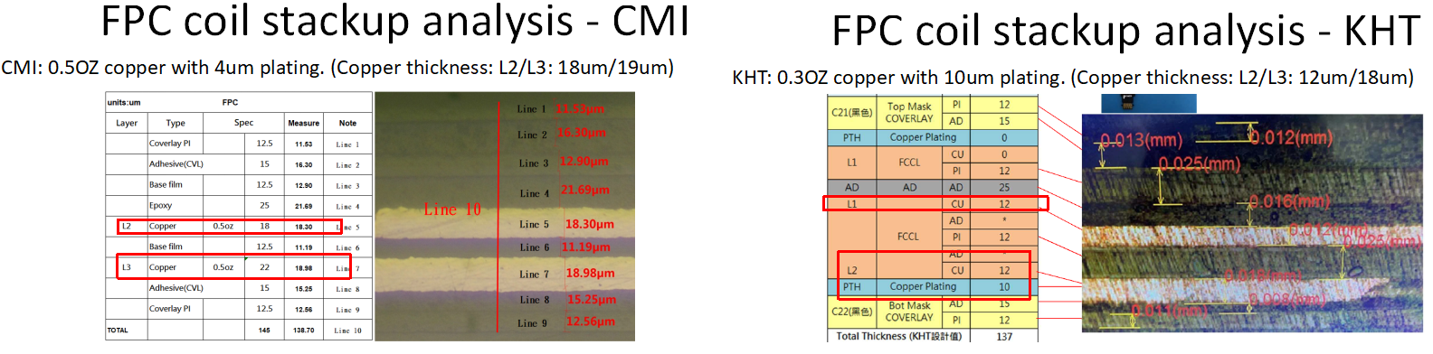
1. We use LDC tool run FEMM with below parameters and get sensor frequency with target is 12.32MHz, but we use oscilloscope probe to measure IN0 cap and the frequency is ~8Mhz, we check our real coil trace width/gap and distance with metal, all are match our design value, so do you know why there is huge different between design and actual value? And is it mean the other calculated parameters like Rp and Q it's value also will not the same with design? 

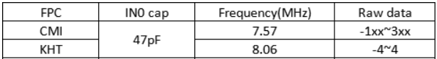
2. Since we have second source FPC vendor KHT(our coil is on FPC), and with them the raw data is stable, but when we change IN0 cap to another value, second source's value become unstable as below table, so I want ask what is the principle of LDC2112? Because the MCU DC-DC switching frequency is 8MHz, so if we tuning LDC2112 resonant frequency far away from 8MHz, the unstable situation should disappear? Or no matter how we tuning resonant frequency, if 8MHz radiation exist, the LDC2112 raw data must be unstable?

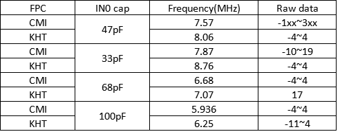
3. If we tune Ccom value(by above, if we tuning Ccom value within 0.3~3.2nf), will it improve this unstable situation? What parameter will be effect when modify Ccom?

Thank you~~

Poki 

  • Poki,

    Thank you for your inquiry and your interest in TI products.

    I will look into your questions and reply by Wednesday.

  • Poki,

    1. What do the connections look like between the sensor and the input pins?
      If they are long, parasitics may be the reason for the difference between the design and the measured frequencies. 
      This can in turn affect the Rp and Q, which can impact the needed IDRIVE.
      The long traces can also pick up external signals, which is why we usually recommend the FDC1004, which has an active shield driver.

      Equipment probes can have parasitics, which are usually known. If the probe parasitics are large enough, the probe could contribute to the lower measured frequency compared to the designed frequency.

    2. We are not sure what to advise, since your question seems to be related to your system and board design. 

    3. The device data sheet advises the Ccom value to be:
      100 × CSENSORn / QSENSORn < CCOM < 1250 × CSENSORn / QSENSORn

  • Hi John:
    1. So you mean with proper design, the calculated and actual value should be the same right?
         a. The distance between IC and coil is 25.3mm (8.8mm on PCB and 16.5mm on FPC with ZIF connector connection), we have let you review our design before on E2E (topic                            LDC2112:LDC2112 EVT SCH and layout review), is this distance and layout ok?

         b. If calculated and actual value is different, how do we know what our real Rp and Q?
         c. We use Tektronix probe TAP1500 which it's cap value <1pf, will it cause measured frequency lower than real?

         d. Increase trace width can reduce parasitics? Below picture is present layout, trace width is 8mil, so should we increase it as large as possible?

         e. Since we will add ground shielding to isolate radiation(below picture area 14.097x10.537), adding this will effect f, Q and Rp? If yes, how do we calculated them?

    2. Simply said, if there is 8MHz noise radiation to coil, how do we design our coil resonant frequency?


    3. I mean if calculated Ccom range is 0.3~3.2nf, what the different we put 0.3nf and 3.2nf? I already do put 1nf and 2.2nf and the      resonant frequency no different


    Thank you~~
    Poki

  • Poki,

    There are several factors that can contribute to the measured frequency being different from the design frequency.
    It can be caused by PCB layer tolerances, PCB trace parasitics & tolerances, component variations, etc.

    Instead of changing Ccom, would it practical for your design if you changed the sensor capacitance to get the resonant frequency you need?

  • Hi John:

    1. How do we avoid those tolerances/variations to get same result with calculated and actual?

    2. Do you think our IN trace length ok? And increase IN trace width can decrease parasitic?

    3. If we can't avoid different between calculated and actual, how do we know our actual Q and Rp? Can we calculated them from actual f?

    4. By your asking "Instead of changing Ccom, would it practical for your design if you changed the sensor capacitance to get the resonant frequency you need?", That I want to know, we already modify different sensor capacitance as above table, but the raw data is not stable, so I want to know if there is 8MHz radiation from other , what the actual resonant frequency that we need to let our raw data stable? As far 8MHz as good or any else?

    5. Could you help check We use Tektronix probe TAP1500 which it's cap value <1pf, will it cause measured frequency lower than real?

    Thank you~~

    Poki

  • Poki,

    I am working with the other members of my team to get answers to your questions, and will have an update tomorrow.

  • Hi John:

    Since there is big different between FPC vendor CMI and KHT, KHT has better performance as below

    We check their stack up as below, their two layer thickness is different, CMI is 18/19 and KHT is 12/18

    Since top side is facing PCB(MCU) and bot side is facing metal, is it possible KHT it's layer facing PCB is much thinner than CMI so MCU radiation effect is smaller than CMI?

    Thank you~~

    Poki

  • Poki,

    Please keep us updated on your troubleshooting efforts as you move forward.