This thread has been locked.

If you have a related question, please click the "Ask a related question" button in the top right corner. The newly created question will be automatically linked to this question.

LDC1101: Configuration and read (MISO) data sensor

Part Number: LDC1101

Hallo everyone,

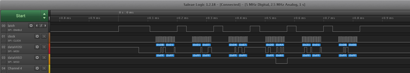
I am trying to configure the LDC1101 chip via SPI protocol using a MSP430 microcontroller. The main goal is to read the LHR data contained in it. I send the configurations via 2 bytes containing address and data. Unfortunately, the registers seem to remain unchanged and I do not receive response; any signal on the MISO pin. Does anyone know where I am wrong, or if something is missing in the code? What I need is simply to get the data from the sensor...

ps. Then I post the signals of the logic analyzer and my code

Thank you very much.

#include <msp430.h> 
#include <rf430frl152h.h>
#include <stdio.h>

void spiConfig();
void regSettings();
void TI_CC_SPIWriteReg(char addr, char value);


volatile char received_ch = 0;
/**
 * main.c
 */
int main(void)
{
    WDTCTL = WDTPW | WDTHOLD;                       // stop watchdog timer

    spiConfig();

    regSettings();
                          

    return 0;
}

void spiConfig()
{
    UCB0CTLW0    |=  UCSWRST;                       //reset, if not..config is not possible

       /*************************************************************
        * ---------- configuration of SPI interface MSP430 ----------
        ************************************************************/
       P1OUT       |=  0x08;
       P1DIR       |=  0x08;                           // Enable, output direction
       P1SEL0      |=  0x07;                           // CLK, MOSI, SOMI, CS option select registers
       P1SEL1      &=  ~0x07;
       UCB0CTLW0   |=  UCMST | UCSYNC | UCMSB ;// 4 pin(mode_3), 8 bit SPI mstr, MSB first
       UCB0CTLW0   |=  UCSSEL_2;                  // SMCLK as clock source
       UCB0BR0     |=   0x02;
       UCB0BR1     |=   0;

       UCB0CTLW0   &=  ~UCSWRST;                       // init USCI state machine by pulling the reset low, "ENABLE spi"

}

void regSettings()
{
    /**********************************************************************************
     * --------- configuration for LDC1101, send data needed to configure it ----------
     *********************************************************************************/

    // !! sleep mode needed to configure the LDC chip !!
    TI_CC_SPIWriteReg(0x0B,0x01);


    // Only LHR measurement
//    TI_CC_SPIWriteReg(0x05,0x01);//shutdown,reset register
//    TI_CC_SPIWriteReg(0x0B,0x02);//shutdown, clock low
//    TI_CC_SPIWriteReg(0x0C,0x01);

    // Read LHR only
//    TI_CC_SPIWriteReg(0x0A,0x20);

//    TI_CC_SPIWriteReg(0x32,0x00);//LHR offset
//    TI_CC_SPIWriteReg(0x34,0x00);//LHR config reg
//    TI_CC_SPIWriteReg(0x3E,0x00);//device value
//    TI_CC_SPIWriteReg(0x3F,0x00);//device ID

    // Register settings for LHR application
    TI_CC_SPIWriteReg(0x01,0x07);
    TI_CC_SPIWriteReg(0x04,0xE7);
    TI_CC_SPIWriteReg(0x30,0x4A);
    TI_CC_SPIWriteReg(0x31,0x01);


    /***********************************************
     * --------- sensor DATA transmission ----------
     **********************************************/

    // command to request MISO LHR data ??
    TI_CC_SPIWriteReg(0xB8,0x00 ); // read register LHR command, reg 0x38


    // !! return to conversion mode !!
    TI_CC_SPIWriteReg(0x0B,0x00);

}

void TI_CC_SPIWriteReg(char addr, char value)       //first byte is register, second byte is data
{
    P1OUT       &=  ~0x08;                          // CS enable by pulling CSn low

    UCB0IFG     &=  ~UCTXIFG;                       // Clear flag
    UCB0TXBUF   =   addr;                           // send Address by putting in SPI buffer
    while(!(UCB0IFG & UCTXIFG));                    // Wait for TX to finish (status byte receive)

    UCB0IFG     &=  ~UCTXIFG;                       // Clear Flag
    UCB0TXBUF   =   value;                              // Send data
    while(!(UCB0IFG & UCTXIFG));                    // Wait for TX to finish (status byte receive)
    __delay_cycles(10);

//    UCB0IFG     &=  ~UCRXIFG;
//    received_ch = UCB0RXBUF;
//    while(!(UCB0IFG & UCRXIFG));                    // Wait for TX to finish (status byte receive)

    P1OUT       |=  0x08;                           // Pull CS high to disable SPI

    //__delay_cycles(100);

}

  • Hi Giuliano,
    We've got your request. We will get back to you as soon as we can.

    Best Regards,
    Bala Ravi
  • Thanks a lot.
    I've been looking for a solution for 2 weeks now but I don't get good results.

    Let me know. Best Regards,

    Giuliano
  • Hi Giuliano,
    Your register settings look good. But as you can see from the datasheet, a first bit of 0 is for writing data and 1 is for reading data. Since your MOSI commands are always starting with 0, you're not reading anything back in the MISO. Please let us know if you need any further assistance. We usually do not support code, but feel free to ask any application or hardware questions.

    Best Regards,
    Bala Ravi
  • Hi Bala,

    Thanks for the reply.

    I was able to read the SPI signals of the EVM LDC1101 module through a logic analyzer and tried to recreate the same protocol.
    That's right, if the first bit is at 0 it means that we are in WRITE mode. In fact, these first bytes in the screenshot I posted, represented the configuration of the LDC1101 chip. They need to be WRITE mode (In EVM, it's the same thing).

    After that, the data is read out. Here I don't understand if I have to expect the automatic response of the LDC1101 sensor or if I still have to send bytes but this time in READ mode.

    So, I should get or create a 5-byte data packet as follows in the image. In case I don't do anything, I don't get anything. In case I send packets with address (READ mode) on MOSI, I always get the MISO signal without information.

    Best regards,

    Giuliano

  • HI Giuliano,
    That's right make sure the first bit you send is 1 to read something back. Also the master has to send a byte to receive a byte. Transmitting a dummy byte (with first bit = 0), is a typical way to make a read transaction. We do not support code anymore, but I was able to find an example code ( I haven't tried it personally), it could be useful to you. Here is the link: www.ti.com/.../snoc032. I hope this helps!

    Best Regards,
    Bala Ravi
  • Hallo Bala,
    I already have the GUI for the EVM LDC1101. But there are no codes available. Did you send me the wrong link? What I might need is really the code that was made for the EVM LDC1101. In this way I could understand where I am wrong in the communication and configuration through SPI between microcontroller and LDC1101 sensor.

    Thank you very much.
    Best Regards,

    Giuliano Cairoli
  • HI,
    I've just found a solution. The problem has been related to the SPI Mode. In my code the configuration was good but apparently wrong for the logic analyzer. So, I was not able to see something on MISO pin.

    Thank you for support me.

    Giuliano Cairoli