This thread has been locked.

If you have a related question, please click the "Ask a related question" button in the top right corner. The newly created question will be automatically linked to this question.

TMP116: Thermal pad isolation issue

Part Number: TMP116

Hello,

I selected TMP116 as the choice of temperature sensors for a circuit that required measuring temperatures on the PCB copper pads at three different points.

So I soldered the thermal pad of the IC to respective PCB copper pads.

However, I found that two of them keep getting damaged. 

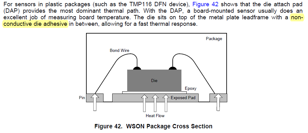
After lot of work I found that the TMP116 pad is not electrically isolated although it claims in the datasheet this is the case (see the attached figures). It says there is a non-conductive die-adhesive between the pad and the die.

I found that when the thermal pad is positively biased with respect to the ground pin, the path breaks when you go above 2-3 volts and start conducting with a diode behavior.

I have tested the IC on my PCB to figure out the problem.

Then, to make sure, I used two new ICs and had them separately biased as I mentioned above and see what happens (without the PCB). Both of them starts a being conductive after the bias goes above 2-3 volts. the current starts around  100 mA and goes up to 500 mA around 3V.

Could you please tell me why the pad behaves this way (showing no isolation) and if if TI has used TMP 116 is such situations?

Thank you very much.

-Nirmana Perera

  • Hello Nirmana

    Thanks for taking the elaborate steps of working to find the potential cause. One question When the external 2-3V is applied, is the current of 100 mA seen on the supply to the thermal pad and/or is there a change in current on the supply rail as well to the TMP116
  • Hi Amit,

    Thank you for your prompt reply.

    As for your question, in the separate test, the sensor was not powered up all. Only the thermal pad and the GND pin were used.

    So the current was the supply to the thermal pad only.

    Thanks,

    Nirmana

  • Hello Nirmana

    Thanks for the information requested. When you mention that the device is damaged, what type of damage are you referring to?

    1. There is a faulty reading.
    2. Device does not communicate.
    3. Excessive current on supply... etc

    If the bias voltage on the thermal pad is somehow "removed" say by grounding the thermal pad, is the damage reversed till the condition appears again?
  • Hi Amit,

    The answer is option 3. The IC is not supposed to draw any current through the thermal pad as it should be isolated as said in the datasheet.
    In my actual circuit, the thermal pads are soldered (electrically connected by choice) actually to a point of the circuit where there is higher potential than the common ground where the GND pin of the sensor is connected. My application requires this.

    And to answer your other question, the damage is still there (there is a still diode type of connection from the pad to the GND terminal), but you wouldn't see it since now there is no bias as the pad and the gnd share the same voltage.
    But it would not answer my issue as the thermal pad needs to be connected to a point with higher potential for my application.
  • Hello Nirmana.

    I understand. But what I would like to know is if because of the issue the device is giving incorrect readout or device is not functional at all? To me that is a damage on the TMP116 device.
  • Hi Amit,

    Thank you again.
    I understand your question.
    Well, two times, after the thermal pad became conductive, the device was sill giving the correct reading through I2C.
    But there was another instance (with another try with a new device), after the pad became conductive, I was reading an incorrect value of 256C all the time. The value did not change. But I'm not sure if the device was still working properly. according to my code, the I2C would become non-responsive if the device is fully damaged. But it seemed responsive as I read a value, but it was of course wrong.
  • Hello Nirmana,

    Thanks for being patient. Now as per the datasheet we do mention that the die adhesive is non-conductive and I am working with the team to better understand the nature of this adhesive in light of the issue you are seeing.

    At the same time the datasheet also mentions that the thermal pad should be left floating or connected to GND, which is a recommendation from TI and is is possibly not taken into consideration on your design.
  • Hi Amit,

    Thank you very much for taking your time for this.

    Yes, I do understand what you mean by the second point.

    However, I figured since the adhesive was non-conductive, I could use TMP116 for my application.

    Anyway, I will be looking forward to hear what you and the team find out about the adhesive and if we can find a solution that might work for my particular application.
    Thank you.

  • Hello Nirmana

    So, if I get it right, the thermal pad is currently connected to a trace which is not at GND nor is floating, but somehow connected to a live potential. If you can send me snapshot(s) of the layout showing how TMP116 is connected, it would helpful.
  • Hi Amit,

    Yes, you are correct.

    The pad is actually electrically connected to a switching node of an inverter leg setup. I want to measure the temperature near the switching node.

    I've attached a simple diagram showing the basic circuit setup.

    Thanks,

    Nirmana

  • Hello Nirmana,

    If it is possible, then I would suggest cutting the top trace to the thermal pad and instead using a thermal silicone pad like the following two join the two sides of the cut trace.

    www.amazon.com/.../ref=sspa_dk_detail_1
  • Hi Amit,

    Thank you very much for your help.
    I will have a look at a solution like this for the moment.
    It will be a bit difficult as it is a 4-layer circuit and I'm afraid of damaging the internal layers.
    But I will give it a try.

    I suppose TI does not have, at the moment, any temperature sensor solution that has kind of isolation I require. I'm thinking about my next revision of the circuit boards.

    Thank you.
  • Hello Nirmana,

    It should not be that difficult to cut the trace path with a sharp blade and not too much pressure to avoid internal plane damage (or potential short.
  • Hello Amit,

    Thank you very much for the feedback, I will try it.

    Best,
    Nirmana
  • Hello Nirmana,

    I got feedback from the team on the issue you were seeing. Under applying a sustained voltage, the thermal pad may conduct as what you are seeing. Hence the recommendation to leave it floating or connecting it to Ground. Also this is not an outlier.

    Secondly, any update on the workaround that was suggested. I am marking the post closed for the moment, but if you have feedback, please post an update.