This thread has been locked.

If you have a related question, please click the "Ask a related question" button in the top right corner. The newly created question will be automatically linked to this question.

DRV5033: Output voltage falls for a moment

Part Number: DRV5033
Other Parts Discussed in Thread: DRV5032, , DRV5021

Dear all,

Our customer would like to know the cause of following phenomenon.

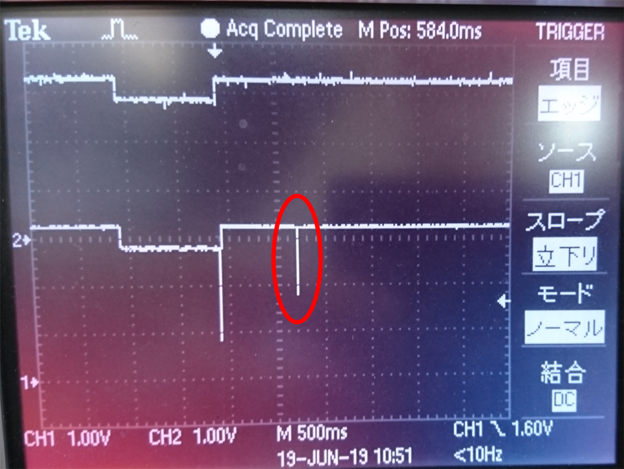
When the power supply voltage is changed from 2.8V to 3.3V in the DRV5033DU, The voltage of OUT terminal (No.2 pin) falls for a moment like figure below.

(upper signal:power supply voltage   Lower signal:voltage of OUT terminal)

Could you tell me the possible cause?

※Our customer says that This phenomenon does not occur with DRV5032FC.

It would be great if you could let me know your thoughts on the following questions.

Best regards,
Y. Ottey

  • Hello Ottey-san,

    Thank you for using the TI forum.  In your question, I believe when you typed DRV5033 you meant DRV5032.  I have a couple ideas of why this could be happening. 

    First, make sure you have a bypass capacitor from VCC to GND (0.1µF min).  This capacitor should be placed close to the device.

    Second, the DRV5032DU and DRV5032FC have different output types.  The DRV5032FC is open-drain output, while the DRV5032DU is push-pull. With the push-pull architecture (figure 15 in the datasheet), it is possible that if VCC changes suddenly that the voltage difference from the output control line to VCC causes the output state to temporarily change until the control has had a chance to update.  You could test this by changing VCC from 2.8V  to 3.3V very slowly and seeing if there is still a problem.  

  • Hi Mitch.

    Thank you for your reply.

    The DRV5033DU is wrong, and it is DRV5033 that the phenomenon is happening.

    DRV5033 is open-drain output type.

    Will the cause or action you answered in the last reply change?

    Could you give me some additional advice?

    Y.Ottey

  • Hello Ottey-san,

    Ok, thanks for the clarification.  The responses above could all still be reasons, only a few things change for the second reason.  Looking at the Functional Block Diagram in section 7.2, it is the "Gate Drive" that is controlling the if the device gets pulled low (instead of the "Output Control". I also recommend looking at the GND to make sure there are no spikes there. 

    I will reach out to the design team to see if they have any additional comments or insights to what you are seeing.

  • Hello Ottey-san,

    I have talked with the designers, and have some more info for you. 

    When this device is powered with a low VCC (ie, near 2.5V), an internal LDO is susceptible to an unstable supply.  This is essentially why you are seeing your output affected when you change the voltage quickly at the low voltage values. 

    The designer gave 2 suggestions.  

    1) Make sure that VCC is clean (this usually requires a stronger power management IC, or in your case not fluctuating VCC)

    2) Raise VCC, for example even to 3.3V or 5V can usually be enough to compensate for the noisy supply.

  • Dear Mitch

    Thank you for your good advice.

    I understood the specification of DRV5033.

    In addition, I would like to ask more question.

    1. For example, when Vcc is changed quickly from 2.8 to 3.3 V, how long does it take for the output to change properly?
    2. My customer seems to control Vcc by microcomputer, so I can not change Vcc slowly. Is there any other way to deal with this other than raising the voltage value of Vcc used?Also, do you know any application that controls the Hall sensor Vcc with a microcontroller?

    Regards,

    Y.Ottey

  • Hello Ottey-san,

    If you consider the voltage change as a turn-on event, then "Power-on time" parameter could be a good guideline for when the output is valid:

    One other possible solution would be to change components to a low voltage Hall so that you don't have to worry this problem.  Based on your application, maybe you may want to look into the DRV5032 or the DRV5021.

  • Dear Mitch

    Thank you for your reply.

    We have confirmed to the customer about GND that you were saying, and confirmed that bypass capacitor from VCC to GND (0.1 μF min) is placed near the device.

    I would like to ask additional questions below.

    1.If DRV5033 is replaced with DRV5032FC (Package: SOT-23) in the same environment and circuit, what happens?

    Also, does the phenomenon change due to product variation?

    2.You mentioned the following before.

    ”When this device is powered with a low VCC (ie, near 2.5V), an internal LDO is susceptible to an unstable supply.  This is essentially why you are seeing your output affected when you change the voltage quickly at the low voltage values. 

    Does the above content occur with DRV5032 FC?

    Customers say that the phenomenon mentioned in the first post does not occur in DRV5032FC, so please let me confirm.

    Regards、

    Y.Ottey

  • Hello Ottey-san,

    Here are my responses to your questions:

    1)  The DRV5032FC can replace the DRV5033 (and is pin to pin compatible). The DRV5032FC is a higher sensitivity, so it will trip sooner than the DRV5033.

    2)  Correct, the above phenomenon should not happen with the DRV5032.

  • Dear Mitch

    Thank you for your reply.

    I would like to ask 2 questions against your previous answer.

    1.You said that the above phenomenon should not happen with the DRV5032 in your reply.

      Can you guarantee this?

    2.Our customer also would like to know the cause of the drop in the red circle in the figure below.

       Could you tell me the possible cause?

      Also, is the same phenomenon likely to occur with DRV5032FC?

    Regards,

    Y.Ottey

  • Dear Mitch,

    As mentioned above, the customer is urged to answer quickly.

    I would appreciate it if you could get back to me right away.

    Regards,

    Y.Ottey

  • Hello Ottey-san,

    Here are my responses to your questions:

    1) We can only guarantee what is in the datasheet, but we have not seen this issue with the DRV5032, and it does not have the LDO setup that was causing the phenomenon in the other part at low voltages. 

    2) The drop in the red circle is most likely from the same issue as the initial drop, which is is related to the VCC voltage level and stability.  A sudden change can cause this, but also a noisy supply. 

    No, the same phenomenon should not exist with the DRV5032FC.

  • Hi, Mitch

    Thank you for your reply.

    I'd like to organize information, so let me ask you some questions about your answers.

    1.I think that this phenomenon does not occur in DRV5032FC because it is the difference of the internal    circuit compared with DRV5033.
    Which of the following is the reason why the problem does not occur with DRV5032FC?

          A: Because the internal LDO installed is different 
          B: Because the sensing circuit configuration behind the internal LDO is different

    2.You answered the following about the second drop.

    The drop in the red circle is most likely from the same issue as the initial drop, which is related to the VCC voltage level and stability.A sudden change can cause this, but also a noisy supply.

    This drop occurs 500 ms after the rise of Vcc. Does this mean that the value of OUT is not stable even after 500 ms?

    Contrary to what you told me before, it took typ. 35 μs to stabilize after Vcc rises.

    3.As the cause of the two dips this time, you answered that Vcc is being used around 2.5 V and that you are changing Vcc suddenly. Which one is more significant?

    Regards,
    Y.Ottey

  • Hello Ottey-san,

    Here are my responses to your questions.

    1) The DRV5032 has many internal differences compared with the DRV5033 because it was designed with an entirely different focus (low power, low voltage).  All of these changes combine cause this phenomenon to not happen in the DRV5032. However, the different LDO is a big part of that. 

    2) The output does stabilize after a typical 35 µs, but this phenomenon is caused by both changes in Vcc and a noisy Vcc when Vcc is very low (around 2.5V).  So, it is likely that the second dip is a result from noise in the supply.  

    3) The low voltage is "more significant" because this phenomenon does not happen at higher voltage.  When at very low voltage (around 2.5V), any fluctuations in Vcc may cause this phenomenon.  These fluctuations could be noise or a change in Vcc.

  • Dear Mitch,

    Thank you for your reply.

    Could I have more questions?

    1. If the Vcc is changed rapidly from 2.8V to 5.0V with DRV5033, do the first and second noise occur?

        And what about 3.3V to 5.0V?

    2. You said that the second dip is a result from noise in the supply.

        To improve the noise of Vcc, it is possible to increase the capacity of the capacitor placed in front of the Vcc pin. Do you have any other advice?

    Regards,

    Y.Ottey

  • Hello Ottey-san,

    Here are my responses to your questions:

    1) It is hard to say exactly if/where the output problem will occur.  And it could be different for each individual device. Going from 3.3V to 5V would be less likely to happen that from 2.8V to 5V, but still could be possible based on various factors, such as supply noise.  

    2) A capacitor can help, and I recommend you use one right next to the Vcc pin.  Sometimes people will even use multiple capacitors of different sizes right next to the Vcc pin to help with noise.  I also recommend that your supply itself has a clean output.  

    In general, since you seem to only be going to 5V, the DRV5032 may be a better fit for your application.