This thread has been locked.

If you have a related question, please click the "Ask a related question" button in the top right corner. The newly created question will be automatically linked to this question.

IWR6843ISK: DMM Interface Pin Muxing

Part Number: IWR6843ISK

Hi Vivek ,

Can you give me more details about DMM interface pin muxing ? Because we got some pin conflict issues .

here are my questions below :

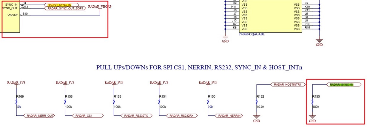
1、Is  the EN(NDMM_EN) N13 or N5  DMM signal necessary ? we don't find this signal on J3 (60PIN HD Connector)of DCA1000  .

2、N13 is currently in use by JTAG, pin TDO .How to deal with this pin ? 

Thank you ,
Simon

  • Simon,

         Which device you are interfacing to DMM? Currently DCA1000 will not support DMM interface.

    Thanks and regards,

    CHETHAN KUMAR Y.B.

  • Thanks  for your quickly reply .

    Now we are gong to build a HIL system based on Altera FPGA .However that is still a challenge for us though we can take TRM for reference .
    we are confusing a bit about how to write external data to ADC buffer .we'll appreciate it if you could help us about this interface .Is there any design  we can refer to ?

    Regards ,
    Simon

  • Hello  , Any update ?

  • Simon,

       Currently we do not have any reference design built for DMM module.

    Technical reference manual has a chapter (Chapter 19) exclusively for DMM module. This chapter provides all the timing relationship for the DMM signals and register details for programming the hardware.

     What is the problem you are facing in this interface? 

    Thanks and regards,

    CHETHAN KUMAR Y.B.

  • CHETHAN KUMAR Y.B. ,

    Q1 : DMM interface on the chip has two modules operation now :

    • Trace Mode
    • Direct Data Mode

    which one shoud I use ?

    Q2 : When I finish wirte a chirp sample data into ADC ping buffer (address : 0x2100 0000), should I toggle DSS_REG.DMMSWINT1.DMMADCBUFPINPONSEL to switch to pong buffer with DSS core ?

    Regards,

    Simon

  • Hello  any information ?

    Thanks,
    Simon

  • Hello,

    Q1 :  Yes, DMM interface on the chip has two modules operation, For hardware in loop function you would need to use Direct data mode. 

    Q2:  Please refer to below block diagram for the DSS_REG.DMMSWINT1.DMMADCBUFPINPONSEL  (Please refer to TRM chapter 13)

    http://www.ti.com/lit/ug/swru522d/swru522d.pdf

    DSS_REG.DMMSWINT1.DMMADCBUFPINPONSEL controls the ADC buffer input path. It need to be configured to "DMM write interface", Otherwise data would be taken from the regular path i.e. Digital front end output or through Test pattern generator depending upon another mux select shown in the diagram. 

    Thanks and regards,

    CHETHAN KUMAR Y.B.

  • CHETHAN KUMAR Y.B.

    I have the follow configurations on the chip :

    1、Select the source of ADC Buffer to HIL :

    //...
            /*****************************************************************************
             * Open ADCBUF driver:
             *****************************************************************************/
            ADCBuf_Params_init(&adcBufParams);
            adcBufParams.chirpThresholdPing = 1;
            adcBufParams.chirpThresholdPong = 1;
            adcBufParams.continousMode = 0;
            adcBufParams.source = ADCBUF_SOURCE_HIL;
    
            /* Open ADCBUF driver */
            gSrrDSSMCB.adcBufHandle = ADCBuf_open(0, &adcBufParams);
            if (gSrrDSSMCB.adcBufHandle == NULL)
            {
                //System_printf("Error: Unable to open the ADCBUF driver\n");
                return;
            }
    //...

    2、Pin setup for DMM :

        //Setup for DMM 
        Pinmux_Set_OverrideCtrl(SOC_XWR68XX_PINJ13_PADAC, PINMUX_OUTEN_RETAIN_HW_CTRL, PINMUX_INPEN_RETAIN_HW_CTRL);
        Pinmux_Set_FuncSel(SOC_XWR68XX_PINJ13_PADAC,SOC_XWR68XX_PINJ13_PADAC_DMM_MUXIN);
    
        Pinmux_Set_OverrideCtrl(SOC_XWR68XX_PINN5_PADBE, PINMUX_OUTEN_RETAIN_HW_CTRL, PINMUX_INPEN_RETAIN_HW_CTRL);
        Pinmux_Set_FuncSel(SOC_XWR68XX_PINN5_PADBE,SOC_XWR68XX_PINN5_PADBE_NDMM_EN);
    
        Pinmux_Set_OverrideCtrl(SOC_XWR68XX_PINR4_PADBF, PINMUX_OUTEN_RETAIN_HW_CTRL, PINMUX_INPEN_RETAIN_HW_CTRL);
        Pinmux_Set_FuncSel(SOC_XWR68XX_PINR4_PADBF,SOC_XWR68XX_PINR4_PADBF_DMM0);
    
        Pinmux_Set_OverrideCtrl(SOC_XWR68XX_PINP5_PADBG, PINMUX_OUTEN_RETAIN_HW_CTRL, PINMUX_INPEN_RETAIN_HW_CTRL);
        Pinmux_Set_FuncSel(SOC_XWR68XX_PINP5_PADBG,SOC_XWR68XX_PINP5_PADBG_DMM1);
    
        Pinmux_Set_OverrideCtrl(SOC_XWR68XX_PINR5_PADBH, PINMUX_OUTEN_RETAIN_HW_CTRL, PINMUX_INPEN_RETAIN_HW_CTRL);
        Pinmux_Set_FuncSel(SOC_XWR68XX_PINR5_PADBH,SOC_XWR68XX_PINR5_PADBH_DMM2);
    
        Pinmux_Set_OverrideCtrl(SOC_XWR68XX_PINP6_PADBI, PINMUX_OUTEN_RETAIN_HW_CTRL, PINMUX_INPEN_RETAIN_HW_CTRL);
        Pinmux_Set_FuncSel(SOC_XWR68XX_PINP6_PADBI,SOC_XWR68XX_PINP6_PADBI_DMM3);
    
        Pinmux_Set_OverrideCtrl(SOC_XWR68XX_PINR7_PADBJ, PINMUX_OUTEN_RETAIN_HW_CTRL, PINMUX_INPEN_RETAIN_HW_CTRL);
        Pinmux_Set_FuncSel(SOC_XWR68XX_PINR7_PADBJ,SOC_XWR68XX_PINR7_PADBJ_DMM4);
    
        Pinmux_Set_OverrideCtrl(SOC_XWR68XX_PINP7_PADBK, PINMUX_OUTEN_RETAIN_HW_CTRL, PINMUX_INPEN_RETAIN_HW_CTRL);
        Pinmux_Set_FuncSel(SOC_XWR68XX_PINP7_PADBK,SOC_XWR68XX_PINP7_PADBK_DMM5);
    
        Pinmux_Set_OverrideCtrl(SOC_XWR68XX_PINR8_PADBL, PINMUX_OUTEN_RETAIN_HW_CTRL, PINMUX_INPEN_RETAIN_HW_CTRL);
        Pinmux_Set_FuncSel(SOC_XWR68XX_PINR8_PADBL,SOC_XWR68XX_PINR8_PADBL_DMM6);
    
        Pinmux_Set_OverrideCtrl(SOC_XWR68XX_PINP8_PADBM, PINMUX_OUTEN_RETAIN_HW_CTRL, PINMUX_INPEN_RETAIN_HW_CTRL);
        Pinmux_Set_FuncSel(SOC_XWR68XX_PINP8_PADBM,SOC_XWR68XX_PINP8_PADBM_DMM7);
    
        Pinmux_Set_OverrideCtrl(SOC_XWR68XX_PINN15_PADBV, PINMUX_OUTEN_RETAIN_HW_CTRL, PINMUX_INPEN_RETAIN_HW_CTRL);
        Pinmux_Set_FuncSel(SOC_XWR68XX_PINN15_PADBV,SOC_XWR68XX_PINN15_PADBV_DMM_CLK);
    
        Pinmux_Set_OverrideCtrl(SOC_XWR68XX_PINN14_PADBW, PINMUX_OUTEN_RETAIN_HW_CTRL, PINMUX_INPEN_RETAIN_HW_CTRL);
        Pinmux_Set_FuncSel(SOC_XWR68XX_PINN14_PADBW,SOC_XWR68XX_PINN14_PADBW_DMM_SYNC);

    Is that all ? Do I need other configurations on the chip ?Besides ,  I still have no idea where to switch ADC ping pong buffer .

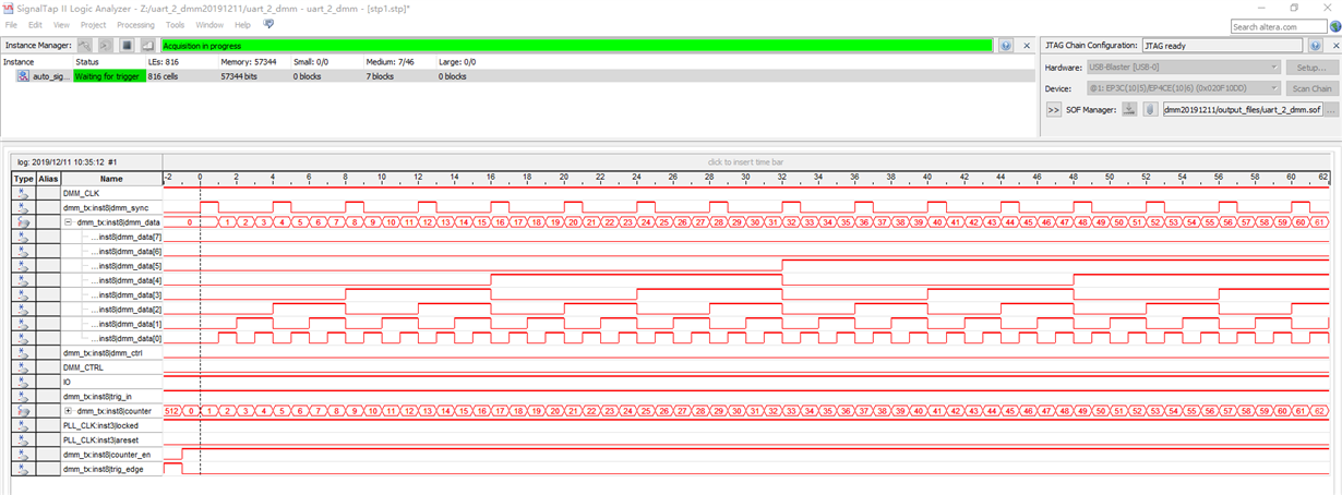
    After these configurations , I got the signal as bellow ,But it's not match with what I sent . I still need to check the FPGA  pin timing :

    Regards ,
    Simon

  • Hello CHETHAN KUMAR Y.B.

    Is this a correct timing for direct  data mode cause I don't find a illustrationin TRM?

    Thanks,

    Simon

  • Simon,

        In the above timing diagram DMM_CLK is not seen, hence timing diagram is not correct.

       Also, There are more steps and sequences need to be followed, Please refer to the attached draft documentation on the DMM interface. For hardware in loop support. 

    Thanks and regards,

    CHETHAN KUMAR Y.B.

  • Simon,

         Please find the attachment in the below link

     /cfs-file/__key/communityserver-discussions-components-files/1023/DMM-interface-V0.3.pdf

    Thanks and regards,

    CHETHAN KUMAR Y.B.

  • CHETHAN KUMAR Y.B.,

    You are the best .That's really helpful!

    Thanks,
    Simon

  • Hi CHETHAN KUMAR Y.B.,
    When we debug the dmm interface ,we have a question below:

    DMM1 in trace mode with dets0 , write 0xfcfff61c with data value 0x5200000 but the ADDR width in the packet are only [17:0] .
    Could you tell me how to do?

    Regards,
    Simon

  • Hello Simon,

         Yes, your understanding is correct,  Address has two components one is base address and another is offset address, for the transfer only offset address is sufficient, Hence ADDR width in the packet are only [17:0],  base address is already set with dets0. 

    Thanks and regards,

    CHETHAN KUMAR Y.B.

  • Thank you CHETHAN KUMAR Y.B. ,

    Follow the doc "DMM Interface V0.3"  , we can write the DMM2_DDMDEST (0xFCFF_F61C) with data 0x5209_0000 finally . However according to the TRM  , ADC Buffer Ping base address should be 0x5200_0000 .

    Are there any updates to the "DMM Interface V0.3.pdf" ? when will TI release the HIL function ?

    Regards,
    Simon

  • Simon,

       Thank you for the confirmation, Sorry for the incontinence you had to go through... 

    ADC Buffer Ping base address is 0x5200_0000, However this is while writing from BSS hardware, hence this address space is read only (You will not be able to write into this space); This is mainly to ensure, this address space is not corrupted while mmWave front end sensor is running mission critical application and this space should not be corrupted inadvertently from other operations.  During Hardware in loop configuration address space would be used 0x5209_0000, during this process BSS would not be running hence it's safe to access it through this interface. 

    I could incorporate this information in DMM Interface document. Currently I do not have timeline when it would be available. This document is draft and undergoing review process and once it's complete we are planning to release on ti.com. 

    Thanks and regards,

    CHETHAN KUMAR Y.B.

  • CHETHAN KUMAR Y.B.,

    We noticed that dmm interface write data in trace mode with dest1 and dest2,but we don't find where to configure the register .
    Could help us to check the psudo code bellow :


    DMM Trace Mode
    DEST0: 0xFCFF_F72C  , Data : 0xFCFF_F700
           0xFCFF_F730  , Data : 0x0000_0009

    DEST1: 0xFCFF_F73C  , Data : 0x5000_0660
           0xFCFF_F730  , Data : 0x0000_0009
     
    DEST2: 0xFCFF_F74C  , Data : 0xFFFF_F94C
           0xFCFF_F730  , Data : 0x0000_0009


    Thanks,
    Simon

  • Hi CHETHAN KUMAR Y.B.,

    Could you help us with the issues about DEST configurations?
    Besides we can't write any data in xWR6843 ES1.0 with DirectDataMode currently and system based on discontinuous clk mode all the timing seems good.
    look forward to your reply.

    Regards,
    Simon

  • Hi CHETHAN KUMAR Y.B.,

    Here are some additional information bellow:

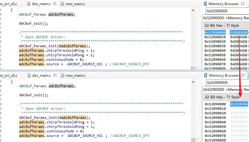
    1、Trying to edit the memory :

    but got an error :

    Cortex_R4_0: Trouble Writing Memory Block at 0x52090000 on Page 0 of Length 0x4: (Error -2130 @ 0x52090000) Unable to access device memory. Verify that the memory address is in valid memory. If error persists, confirm configuration, power-cycle board, and/or try more reliable JTAG settings (e.g. lower TCLK). (Emulation package 8.3.0.00003)
    

    Regards,
    Simon

  • Hello ,Are there any update about DDM issues?

    Regards,
    Simon

  • Simon,

     I see issues in the pseudo code... 

    DEST0: should be part of configuration done by the MSS R4F initial configuration ( By the host application). Also values needs some corrections. 

    You could review below reference Pseudo code

  • Simon,

      Also if the DMM clock is discontinuous then it must be configured accordingly.

    Please refer below section from TRM.

    Thanks and regards,

    CHETHAN KUMAR Y.B.

  • CHETHAN KUMAR Y.B.,

    Yes , we set the CONTCLK to 0 and trace mode works fine .However , there is nothing change at 0x5209_0000 when we write data with direct data mode .

    Q1 : Could you tell me how to know the data are successfully written in the address with DDM?

    Q2 : Before step8 DMM2_DDM(ADC_BUFF PING) , do we need to generate a frame start interrupt  by writing memory 0xFFFFF954 with 0x00000080 ?

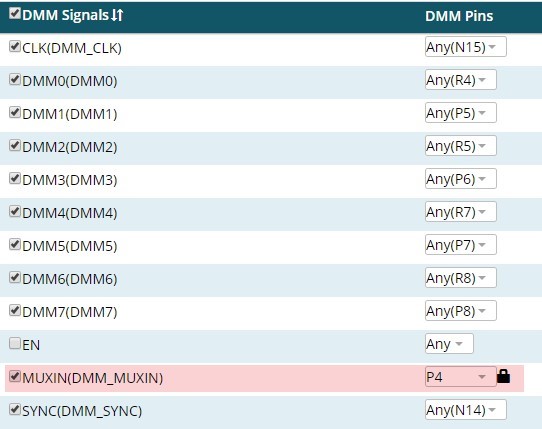
    Q3 : For DMM IO Pin configuration we set SOC_XWR68XX_PINP4_PADBB as DMM_MUX_CTL ,this is a difference from you show me.

    These issues  bothered us for a long time, I really appreciate your help and hope you can provide more information.


    Regards,
    Simon

  • Simon,

        You cannot read from 0x5209_0000 this location this is ADC_buffer write only, To read the content of the written values you could read from the 0x5200 0000 address. 

    Q1 : Could you tell me how to know the data are successfully written in the address with DDM?

    Ans: By reading above address space you could read the written content through the HIL interface. 

    Q2 : Before step8 DMM2_DDM(ADC_BUFF PING) , do we need to generate a frame start interrupt  by writing memory 0xFFFFF954 with 0x00000080 ?

    Ans: If you follow the above procedure not needed, It's handled at later stage in the sequence. 

    Q3: DMM_MUX_CTL has multiples pins from which you could do pin muxing, P4 is also one among them. Could you please send the all the pin config used for this interface? 

    Thanks and regards,

    CHETHAN KUMAR Y.B.

  • CHETHAN KUMAR Y.B.,

    Thanks for your reply . All the pins muxing are as follows:

        /*DMM Interface Configuration*/
        //1、DMM IO Pin Mux
        /* ******************************************************************************
         * Call the Pinmux_Set_OverrideCtrl for each pad to set the input/ouput/hw_ctrl mode
         * For example, for most peripherals, the pads should be put in HW_CTRL mode.
         * ******************************************************************************/
    
        Pinmux_Set_OverrideCtrl(SOC_XWR68XX_PINP4_PADBB, PINMUX_OUTEN_RETAIN_HW_CTRL, PINMUX_INPEN_RETAIN_HW_CTRL);
        Pinmux_Set_FuncSel(SOC_XWR68XX_PINP4_PADBB,SOC_XWR68XX_PINP4_PADBB_DMM_MUXIN);
    
        Pinmux_Set_OverrideCtrl(SOC_XWR68XX_PINR4_PADBF, PINMUX_OUTEN_RETAIN_HW_CTRL, PINMUX_INPEN_RETAIN_HW_CTRL);
        Pinmux_Set_FuncSel(SOC_XWR68XX_PINR4_PADBF,SOC_XWR68XX_PINR4_PADBF_DMM0);
    
        Pinmux_Set_OverrideCtrl(SOC_XWR68XX_PINP5_PADBG, PINMUX_OUTEN_RETAIN_HW_CTRL, PINMUX_INPEN_RETAIN_HW_CTRL);
        Pinmux_Set_FuncSel(SOC_XWR68XX_PINP5_PADBG,SOC_XWR68XX_PINP5_PADBG_DMM1);
    
        Pinmux_Set_OverrideCtrl(SOC_XWR68XX_PINR5_PADBH, PINMUX_OUTEN_RETAIN_HW_CTRL, PINMUX_INPEN_RETAIN_HW_CTRL);
        Pinmux_Set_FuncSel(SOC_XWR68XX_PINR5_PADBH,SOC_XWR68XX_PINR5_PADBH_DMM2);
    
        Pinmux_Set_OverrideCtrl(SOC_XWR68XX_PINP6_PADBI , PINMUX_OUTEN_RETAIN_HW_CTRL, PINMUX_INPEN_RETAIN_HW_CTRL);
        Pinmux_Set_FuncSel(SOC_XWR68XX_PINP6_PADBI,SOC_XWR68XX_PINP6_PADBI_DMM3);
    
        Pinmux_Set_OverrideCtrl(SOC_XWR68XX_PINR7_PADBJ, PINMUX_OUTEN_RETAIN_HW_CTRL, PINMUX_INPEN_RETAIN_HW_CTRL);
        Pinmux_Set_FuncSel(SOC_XWR68XX_PINR7_PADBJ,SOC_XWR68XX_PINR7_PADBJ_DMM4);
    
        Pinmux_Set_OverrideCtrl(SOC_XWR68XX_PINP7_PADBK, PINMUX_OUTEN_RETAIN_HW_CTRL, PINMUX_INPEN_RETAIN_HW_CTRL);
        Pinmux_Set_FuncSel(SOC_XWR68XX_PINP7_PADBK,SOC_XWR68XX_PINP7_PADBK_DMM5);
    
        Pinmux_Set_OverrideCtrl(SOC_XWR68XX_PINR8_PADBL, PINMUX_OUTEN_RETAIN_HW_CTRL, PINMUX_INPEN_RETAIN_HW_CTRL);
        Pinmux_Set_FuncSel(SOC_XWR68XX_PINR8_PADBL,SOC_XWR68XX_PINR8_PADBL_DMM6);
    
        Pinmux_Set_OverrideCtrl(SOC_XWR68XX_PINP8_PADBM, PINMUX_OUTEN_RETAIN_HW_CTRL, PINMUX_INPEN_RETAIN_HW_CTRL);
        Pinmux_Set_FuncSel(SOC_XWR68XX_PINP8_PADBM,SOC_XWR68XX_PINP8_PADBM_DMM7);
    
        Pinmux_Set_OverrideCtrl(SOC_XWR68XX_PINN15_PADBV, PINMUX_OUTEN_RETAIN_HW_CTRL, PINMUX_INPEN_RETAIN_HW_CTRL);
        Pinmux_Set_FuncSel(SOC_XWR68XX_PINN15_PADBV,SOC_XWR68XX_PINN15_PADBV_DMM_CLK);
    
        Pinmux_Set_OverrideCtrl(SOC_XWR68XX_PINN14_PADBW, PINMUX_OUTEN_RETAIN_HW_CTRL, PINMUX_INPEN_RETAIN_HW_CTRL);
        Pinmux_Set_FuncSel(SOC_XWR68XX_PINN14_PADBW,SOC_XWR68XX_PINN14_PADBW_DMM_SYNC);

    Thanks & Regards,
    Simon

  • Hi  CHETHAN KUMAR Y.B.,

    Do you find any mistakes in my pin configuration about this interface ?It  seems good ,cause Trace Mode works fine .

    Regards,
    Simon

  • CHETHAN KUMAR Y.B.,

    First , we can write the test data in 0x5209_0000 with DDM finally .

    However , we still get some issues and hope you can guide us to figure it out.
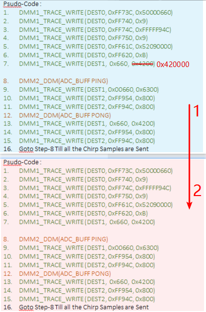
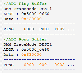
    We follow the psudo-code you provide for us but it seems no data are writen in the address . Then we try as follows:


    1、Follow the step1 to step16 , only change the data in step7 0x4200 to 0x420000 .
    2、Follow the step1 to step16 , do not change the data in step7 0x4200 .
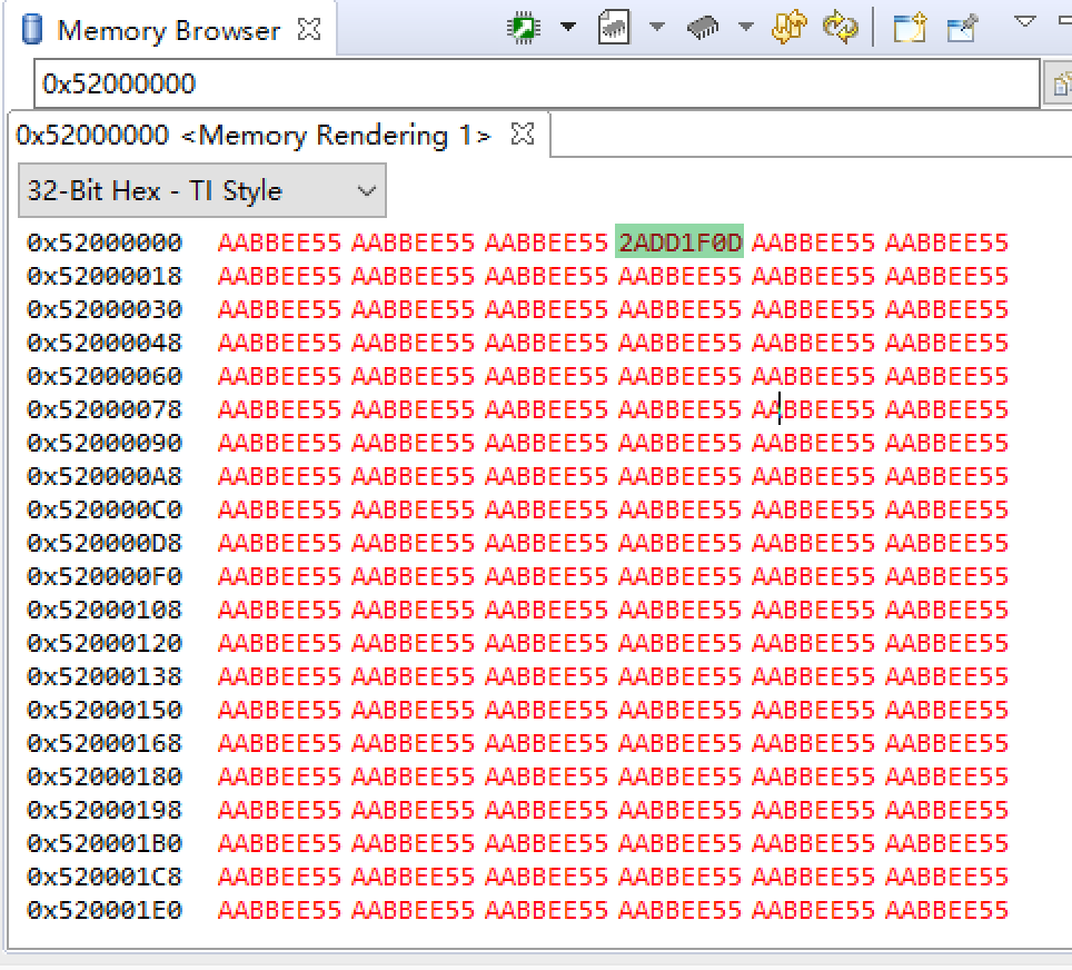
    3、What we get is shown in the picture above but as you can see there is a data error in the green box .


    We have no idea what happened .
    Is there something wrong in our sequence ?

    Looking forward to your help .

    Regards,
    Simon

  • Hi CHETHAN KUMAR Y.B.,

    Any update for my questions ?


    Regards,
    Simon

  • Hello Simon,

        Congratulations for getting the Hardware in loop working on your setup. Thanks a lot for going through above procedure.

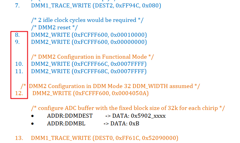
    Also would like to apologize for the typo in above document. Thank for correcting it. As you rightly stated, on the step 7, step 9 and Step 13 need to have lower 16bits should be zero; value expected is 0x420000 during Ping transcation and 0x630000 during pong transaction. I'm referring below TRM section for your reference 


    I have attached the updated correct sequence in the below diagram.

    Thanks and regards,

    CHETHAN KUMAR Y.B.

  • Hello Simon,


    For the wrong value in the memory, My suspect would be in the following  area:

    1) DMM interface clock/Data rates, Could you please let us know what is the interface speed used at. 

    Could you reduce the interface timing by a factor of 2 and see, it has improved? 

    2)  There could be setup and hold time violation on the clock edge to data in the below timing diagram.

    I have referred to your previous timing diagram.

    In the below timing diagram clock not shown; one need to review the setup and hold time for the clock and data should meet the datasheet timing requirements.

    Please refer the datasheet timing specification for the DMM interface. 

    Thanks and regards,

    CHETHAN KUMAR Y.B.

  • CHETHAN KUMAR Y.B.,

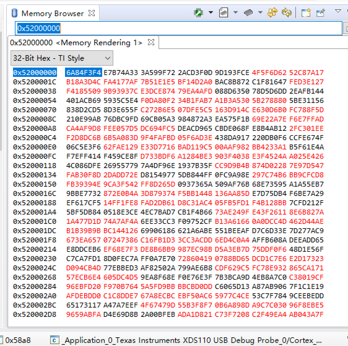
    Thanks for your reply. After writing with the expected value we still get a issue .
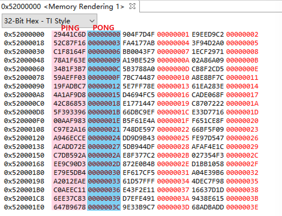
    Here is a screenshot bellow :

    As you can see ,we can write the data from 0000_0000 to 0000_003E  . However , it seems we can't write the expected data into ping buffer . Our test data is as follows:

    we have double checked our code but don't know what happened .
    Could you help about that ?

    Regards,

    Simon

  • Hello Simon,

       Could you please re-check address location of ping buffer?

    Also, could you please confirm what is the value specified for the DDM_WIDTH? 

    Thanks and regards,

    CHETHAN KUMAR Y.B.

  • CHETHAN KUMAR Y.B.,

    Here are some details bellow:

    Regards,

    Simon

  • Hell Simon,

         I'm checking on this, I would need couple of days more to review in detail. 

    Thanks and regards,

    CHETHAN KUMAR Y.B.

  • CHETHAN KUMAR Y.B.,

    Any update for my question ?

    Thanks & Regards 

    Simon

  • Simon,

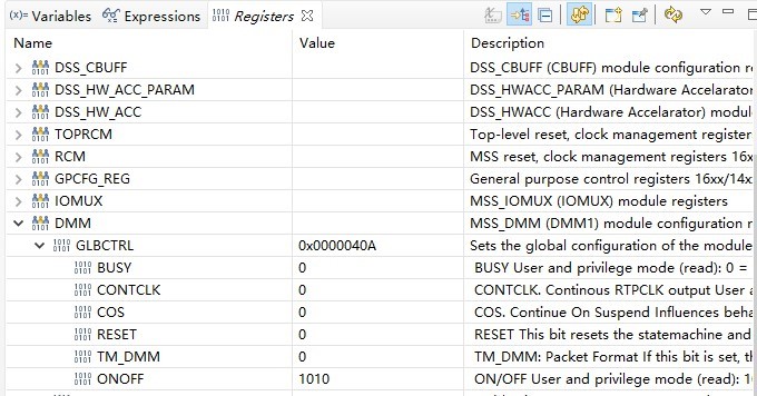
         You may need to reset the DMMs (DMM1 and DMM2) when you switch from Trace mode to DDM modes. 

    Also 2 idle clock cycles would be required whenever there is a transition between the two modes (Trace and DDM mode).

    Thanks and regards,

    CHETHAN KUMAR Y.B.

  • Hi CHETHAN KUMAR Y.B.,

    Thank you for your reply .Could you update the psudo code for me according to your advices?

    Regards ,

    Simon

  • Hello Simon,

       I have updated the psudo code,  Please see below link. 

    /cfs-file/__key/communityserver-discussions-components-files/1023/DMM_5F00_Configuration_5F00_Psudo_5F00_code.pdf

    Thanks and regards,

    CHETHAN KUMAR Y.B.

  • CHETHAN KUMAR Y.B.,

    I'll try this when I back to the office .

    Thanks & Regards,

    Simon

  • Simon,

         Thanks for your confirmation. 

    Thanks and regards,

    CHETHAN KUMAR Y.B.

  • CHETHAN KUMAR Y.B.,

    How are you doing ?
    We added a 2 idle clock delay to the original code ,however we still can't get a correct result because the data in the register is random.. I will attach the simulation wave file for you .

    wave_Lattice_0312.zip


    Besides , we have some questions about the psudo code :

    Q1: DEST0REG1 <0xFCFF_F72C> : 0xF7FF_xxxx   , this value shouldn't it be 0xFCFF_xxxx ?


    Q2: In step 12 , this data 0x5902_xxxx  conflicts with the data 0x5209_xxxx of step 13.We believe 0x5209_xxxx is right one ,right?

    Q3: According to step 8 to step 11 MSS R4 should reset the DMM2 and reconfigure the DMM2 in functional mode ,but how does the R4 core know when to reset the DMM2 ? Is there an interrupt signal?


    Q4: Do you write the data into adc PING/PONG buffer correctly with DMM interface ? Could you provide the right verilog simulation waveform file for us for reference?

    Best Regards,
    Simon

  • Hi CHETHAN KUMAR Y.B.,

    Waiting for your reply.

    Thanks,

    Simon

  • Hello Simon,

        We need sometime to respond to the above question, we will get back to you by next week. 

    Thanks and regards,

    CHETHAN KUMAR Y.B.

  • Hi CHETHAN KUMAR Y.B.,

    I'm really glad to have your reply and I'll wait for your solution.

    Thanks & Regards,
    Simon

  • Any update for my questions?

    Thanks & Regards,

    Simon

  • Hello ?Any information?

    Thanks,

    Simon

  • Hello Simon,

       Sorry for the delay, Please find the answers to the questions about the psudo code

    Q1:  You are right, DEST0REG1 <0xFCFF_F72C> : 0xF7FF_xxxx, should be --- DEST0REG1 <0xFCFF_F72C> : 0xFCFF_xxxx

    Q2:  In step 12, it should be ---- ADDR:DDMDEST  -> DATA: 0x5209_xxxx, there’s a typo in our document.

    Q3: DMM2 is reset every-time when a chirp data is written in ping/pong memory. So using the chirp available interrupt, we can figure that out, and reset DMM2.

    Q4: We could write data into ADC PING/PONG buffer correctly with DMM interface, for different project and different configurations using pattern generator. I do not have verilog simulation waveform file.

    I have update the psudo code based on above feedback. 

    /cfs-file/__key/communityserver-discussions-components-files/1023/DMM_5F00_Configuration_5F00_Psudo_5F00_code_5F00_rev2.pdf

    Thanks and regards,

    CHETHAN KUMAR Y.B.

  • Hi CHETHAN KUMAR Y.B.,

    Thanks for your reply.
    I modify the code as follow , could you check this for us ?

    /**
     *  @b Description
     *  @n
     *      This is the callback function registered with the ADC Driver which is invoked
     *      when a chirp is available. This is executed in the ISR context.
     *
     *  @param[in]  arg
     *      Application registered argument
     *
     *  @retval
     *      Not Applicable.
     */
    static void Mmw_DSS_chirpIntCallback(uintptr_t arg)
    {
        gSrrDSSMCB.chirpProcToken = 1;
        gSrrDSSMCB.stats.chirpIntCounter++;
    	
    	//
    	//6、DMM2 Reset
    	WriteMemory(0xFCFFF600, 0x00010000);
    	WriteMemory(0xFCFFF600, 0x00000000);
    
    	//7、DMM2 Configuration (8 pin pads in Functional Mode)
    	WriteMemory(0xFCFFF66C, 0x000403FF);//8pin
    	WriteMemory(0xFCFFF68C, 0x000403FF);//0x0007FFFF 16pin
    
    	//8、DMM2 Configuration in DDM Mode
    	//    WriteMemory(0xFCFFF600, 0x0004050A);
    	//0x0004050A    ,DMMCLK is expected to be free running between packets.   
    	//0x0000050A	,DMMCLK is expected to be suspended between two packets
    	WriteMemory(0xFCFFF600, 0x0000050A);//DDM_WIDTH = 32bit 
    	//
        return;
    }
    

    Thanks && Gegards,
    Simon

  • Hi CHETHAN KUMAR Y.B.,

    When does TI going to release the new FPGA firmware version that support HIL?

    Thanks,
    Simon

  • Dear Simon,

       On new FPGA firmware to support HIL: I do not have time line.

    The code appears to be correct,  Two Idle DMM clock cycles are required whenever there is a transition between the two modes (Trace and DDM). 

    It’s better to provide two Idle DMM clock cycles, while writing every new chirp and a new frame, hence it is required before DMM2 reset. 

    Thanks and regards,

    CHETHAN KUMAR Y.B.