This thread has been locked.

If you have a related question, please click the "Ask a related question" button in the top right corner. The newly created question will be automatically linked to this question.

IWR6843: ISK Antenna Design Change Question

Part Number: IWR6843

Dear TI,

Good day.

We design a new PCB with re-designed antenna and found some issue which could not be understood.

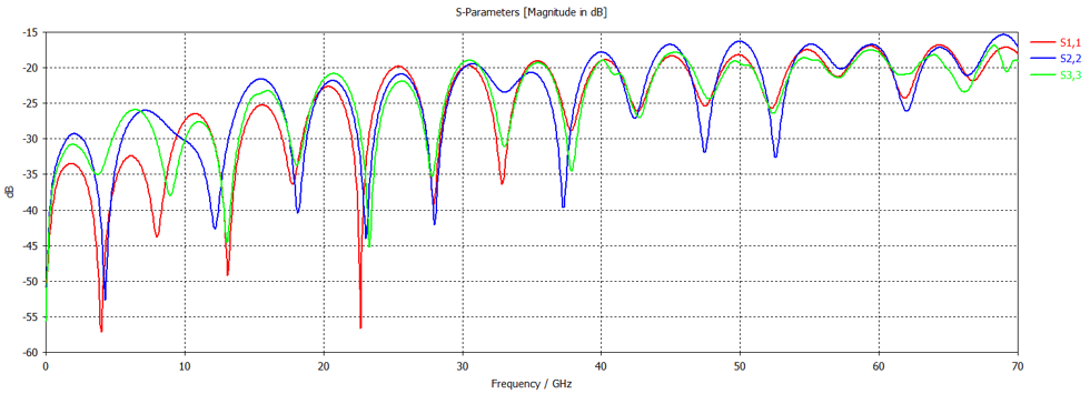
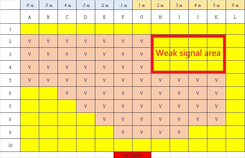
The test results are shown in the below figure. The signal in rectangular area marked by red line is very weak and the TI ISK PCB could not find the same problem. 

We have compared the antenna radiation pattern of TI and ours and could not find the significant differences.

The antPhaseRot is revised because we changed the antenna placement. 

So far we tried to analyze the issue by mmWave_Demo_Visualizer 3.4.0 which and still have no idea about this issue.

Could you please help suggest what kind of experiments we could do to clarify this issue? 

Thanks.

The related information is listed in the below.

 Lab: 68xx_3D_people_counting

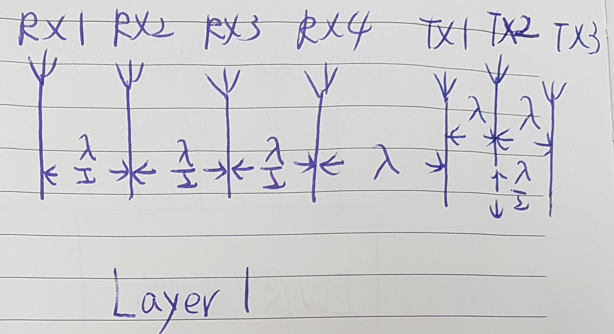
The figure shown below is TI original antenna placement .

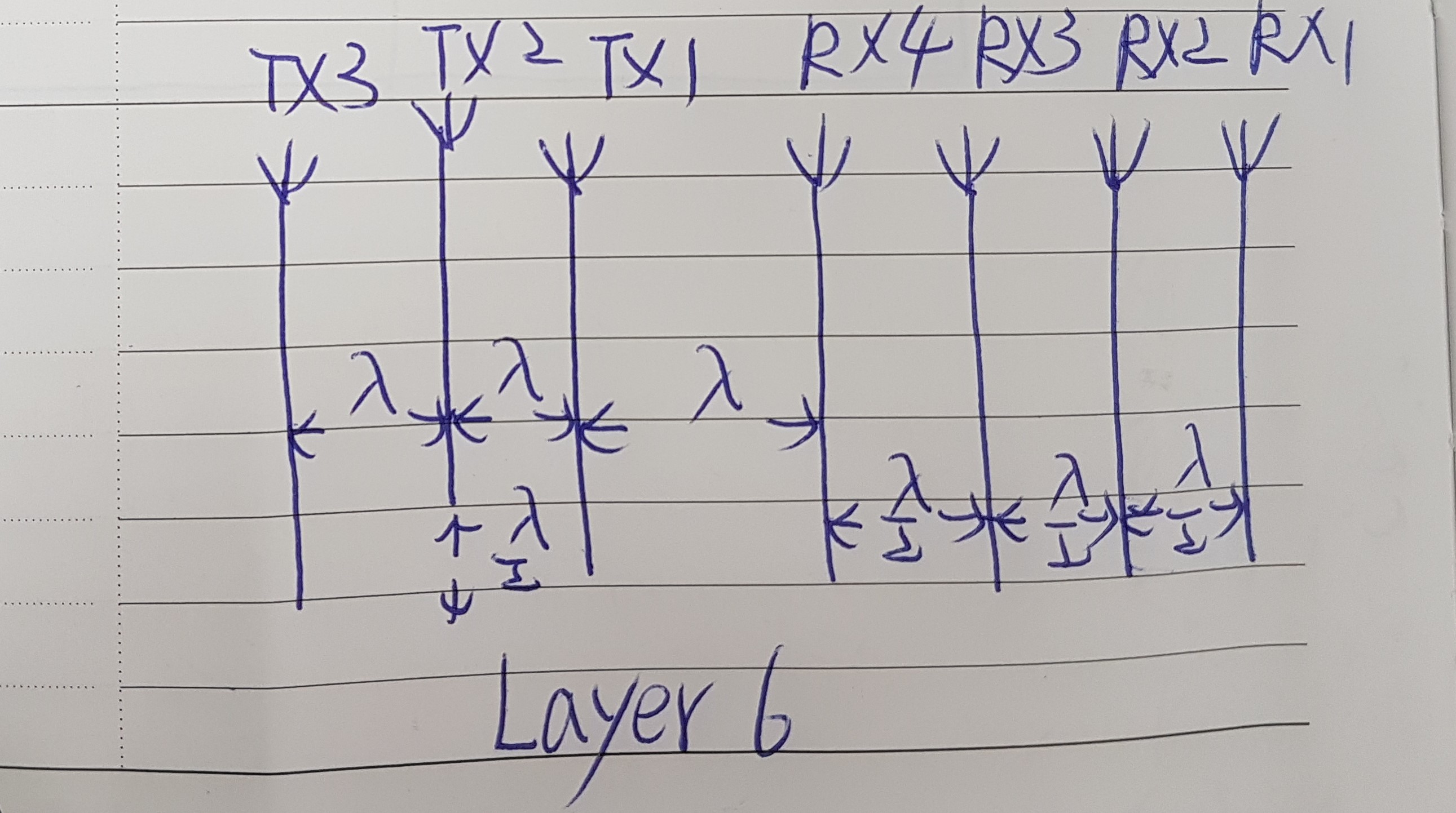
The figure shown below is our antenna placement .

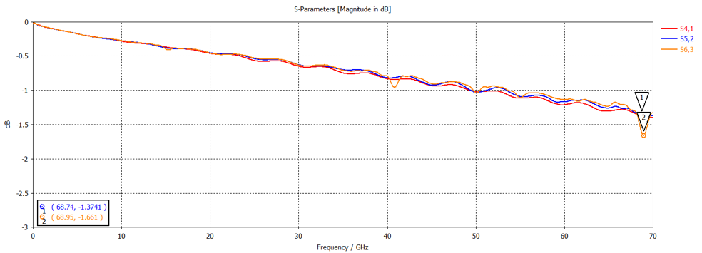
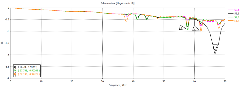
Three antenna test results are shown in the below figure.

Blue line- Our antenna simulation results by CST.

Red line- Our antenna measurement results in anechoic chamber.

Black dotted line-  TI ISK antenna simulation results by CST.


  • Hello user6110370,

        Is the stack-up of the PCB exactly identical as that of IWR6843ISK design. If there are differences could you please highlight the differences that are carried out.

    If there is a change in stackup, there is a possibility of distortion in the antenna radiation patterns? 

    Is it possible to post your Antenna configuration to compare with IWR6843ISK? 

    Thanks and regards,

    CHETHAN KUMAR Y.B. 

  • Dear CHETHAN,

    Good day.

    There  is no difference between PCB stackup.

    Some differences between our PCB and TI's are listed below.

    1. Our RF Trace: width 0.15 gap 0.1

        TI RF Trace: width 0.198 gap 0.203

    2. We remove the below filter which exists in TI PCB.

    3. Difference of antenna placement

    TI Antenna Placement

    Antenna on Layer 1

    IWR 6843 on Layer 1

    Our Antenna Placement

    Antenna on Layer 6

    IWR 6843 on Layer 1

    We will revise the PCB next week.

    We would like to change the antenna design for better performance.

    Please help suggest.

    Thanks a lot.


  • Hello user6110370,

          Stub network is needed to increase the bandwidth of the Antenna, removal of these elements needs Antenna re-simulation on the bandwidth and antenna gain and other parameters. 

    Fundamentally, there is no flaw in your antenna placement, It appears to be mirrored w.r.t to TI antenna placement on EVM.

    For this purpose, have you placed mm-WAVE sensor on top and antenna on the bottom side of the board? "Via"s are not recommended on the Antenna traces. 

    Without looking at the layout it would be hard to comment on Antenna & placement. 

    Also there is change in the RF trace width and Air-gap, This warrants a 3D EM simulation. There are two elements that needs to be looked at

    1) Package to board transition:

    RF trace width/air gap, via fence and ground slot opening under the BGA in Layer 2 (GND) is provided, such that, 50 Ohm impedance is obtained at the edge of the package. If there is a change in the trace width and air-gap there could be problem for the RF transition to board from package.

    2) 50 Ohm grounded CPW transmission line traces have been designed to match 50 Ohm at the package edge and routing all the way to Antenna ports. 

    Hence RF trace-width / air-gap, placement of device, Antenna, matching elements are carefully constructed on TI EVM, changing any of these elements will have adverse affect on the Antenna radiation patterns. If this absolutely need to be changed then careful 3D electro-magnetic simulations are needed.

    Thanks and regards,

    CHETHAN KUMAR Y.B.

  • Dear CHETHAN,

    Good day.

    Yes, we have placed mmwave sensor on top side and antenna on bottom side.

    All RF traces are on top layer and we do not use any via for antenna in different layer.

     Simulation results of RF traces are listed in the below.

    Tx Traces


    S11 of Tx RF Traces

    S21 of Tx RF Traces

    Rx RF Traces


    S11 of Rx RF Traces

    S21 of Rx RF Traces

    1) Package to board transition:

    RF trace width/air gap, via fence and ground slot opening under the BGA in Layer 2 (GND) is provided, such that, 50 Ohm impedance is obtained at the edge of the package. If there is a change in the trace width and air-gap there could be problem for the RF transition to board from package.

    -->There is no change for this part.

    2) 50 Ohm grounded CPW transmission line traces have been designed to match 50 Ohm at the package edge and routing all the way to Antenna ports. 

    Hence RF trace-width / air-gap, placement of device, Antenna, matching elements are carefully constructed on TI EVM, changing any of these elements will have adverse affect on the Antenna radiation patterns. If this absolutely need to be changed then careful 3D electro-magnetic simulations are needed.

    -->Please refer to the simulation results listed above. We also did the measurement on network analyzer and the results are identical.

    For software parts, we just revised the config file(ISK_6m_default.cfg) in 3D people counting lab to fit the antenna placement and phase. We did not  change any DSS code .

    Is it possible related to DSS code because the antenna placement, gain, bandwidth and FOV are changed?

    Thanks.

  • Hello,

       Thank you for sharing the measurement results, from the results it looks fine for the S11 and S21 for the receiver transmission line traces. Is it same for all the Tx lines also? 

    Concern is Antenna traces are in two different layers, This needs careful design of mmWave launch from one layer to other layer (Current IWR6843ISK stackup is not suitable).

    With the current ISK stack-up, top-layer Rogers material and inner layers FR4 materials are present, transition causes not only losses but changes the DK values, which may lead to distortion in antenna radiation patterns.

    Before you could check on the application code, you need to check the Antenna Radiation patterns for all the Tx and Rx pairs are correct or not. 

    You could refer to below link for the radiation patterns. 

    http://dev.ti.com/tirex/explore/node?node=ANS49gohN4gX2.NvHAAGGQ__VLyFKFf__LATEST

    As antennas are changed this would need some changes to Angle-of-Arrival estimation code (either in DSP or Hardware accelerator) in the signal processing operation as well. 

    Thanks and regards,

    CHETHAN KUMAR Y.B.

  • Dear CHETHAN,

    Good day.

    The link could not be opened. Please help check again.

    And for Angle-of-Arrival estimation code, could you please help share the related document?

    Thanks. 

  • Hello,

    You could refer to the below thread to get some pointer on how angle of arrival processing is done in the embedded framework (Using hardware accelerator and DSP) 

    You could refer to be below thread. SDK documentation provides comprehensive documentation on this aspect.

    http://e2e.ti.com/support/sensors/f/1023/p/893446/3317946#3317946

    Thanks and regards,

    CHETHAN KUMAR Y.B.

  • Dear Chethan,

    Good day.

    Thanks for the reply.

    We tried to modify "antenna_geometry.c" but the area of the weak signal still exist.

    Today we found in another lab which called "long_range_people_detection" and the area of the weak signal was disappeared.

    As I know "long_range_people_detection"  use OOB signal chain and "68xx_3D_people_counting" use Capbon Beamforming algorithm.

    Do you have any idea for this?

    Thanks a lot.


  • Hello,

       Do you have the updated detection list as shown above with the long_range_people_detection chain? 

    Long range people detection chain uses beam-forming algorithm to improve the transmitter power (Hence you will notice improved detection quality) by combining multiple transmitters together and it steers the beam to improve field of view..

    You could find more details from the below link

    http://dev.ti.com/tirex/explore/node?node=AHnMTJHTjyhPJEjW5MBXfA__VLyFKFf__LATEST


    Thanks and regards,

    CHETHAN KUMAR Y.B.