This thread has been locked.

If you have a related question, please click the "Ask a related question" button in the top right corner. The newly created question will be automatically linked to this question.

DRV421: Doubts and questions regarding feasibility of RCD (Residual Current Detector) design with DRV421 IC

Part Number: DRV421
Other Parts Discussed in Thread: DRV425, DRV401

Dear Mr. Javiers Contreras,

I hope you are doing fine in these times.

Project Description:

We at DC Opportunities R&D B.V in the Netherlands are developing a RCD (Residual Current Detector) for pure DC grids with ± 360 - 380 V DC mains voltage carrying a ± 10 A current which might vary depending on the load.

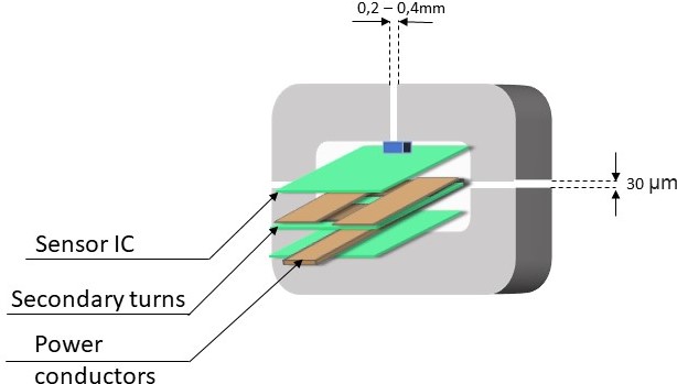
The RCD to be developed is to measure : ± 20 - 30  mA residual or leakage currents. Please find below an image for the idea of the RCD design:


Basically we are considering to place the PCB holding the DRV421 IC and it's circuitat the top just below a 0.4 mm air - gap which just sits on top of the sensor. Goal is to detect the flux (or fringing flux)  jumping the air-gap along the sensor's sensitivity axis.  The other 30 µm cuts are just for the purpose of adjusting the air - gap to 0.4 mm since the cut is usually 1 mm by the manufacturer of the magnetic core. 

The second set of PCBs (~ 6 - 9 PCBs) will contain the secondary windings to provide the reqd. 200 - 300 mH for compensation as recommended in the datasheet.

The last PCB at the bottom consists of the Power Mains - 3 Cu Tracks on adjacent layer namely :  +ve, -ve and Neutral ; the former two poles carrying ± 10 A load current respectively.

The goal is to sense any "differential" current (± 20 - 30 mA) or residual current flowing through these lines and immediately trip the faulty pole or set of poles. This is done by another PCB circuit consisting of a Solid State DC Circuit Breaker which has been built.

Magnetic Core: Core we are using is a Nanocrystalline material with relative permeability (µr) = 30,000 ( + slightly more for DC ).  The core specifications are attached for your kind reference. I made some simulations for a 1 A differential current  in COMSOL Multiphysics 5.3 as below:


                                                                             Fig 1: Geometry used for 2D modeling of Nanocrystalline racetrack shaped magnetic core in COMSOL Multiphysics 5.3 b.


                                                                           Fig 2: Simulation result with a 1 A differential current - Positive Cu trace carrying +11 A and Negative Cu track carrying -10 A respectively and 0A in Neutral.

We get - 360 - 410 µT/A on the "Probe" considered within  the DRV421 PCB. The probe considered is 0.4 mm length and 0.3 mm height sitting within a 0.8 x 4 mm DRV421 sensor.

Below are my doubts and questions on the IC :

Questions:

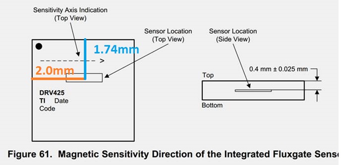
1.    What is the position of the 'Probe' (Fluxgate Front-end sensor) within the Fluxgate IC ? This is requested by us for an accurate simulation on COMSOL. An image representation of what I ask is below:


                                                     Fig 3:  What is the length of probe 'X' and width 'Y' and it's position within the IC:  'X1 , Y1' .

2.    What is the Relative Permeability (µr) of the fluxgate probe or the materia (Soft-iron/ Stell etc.) of the probe ? I ask this because even if the probe has a slightly higher permeability than air, the magnetic flux

        density shoots up to 500 - 600 µT/A.  Making it more sensitive to smaller current changes. Or do we need to consider a 500 µT/mA ?

3.     When we talk about Fluxgate, does the core needs to be 'easily saturable' (around 200 - 500 mT) ? Or we talk about only the Fluxgate Probe which is easily saturated within the DRV421 ? The saturation of this

         core we are using is around 1.5 - 1.7 T because of the material.

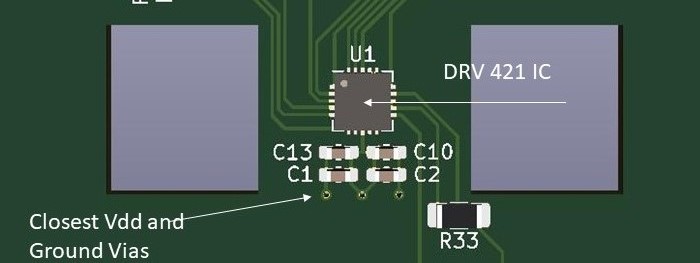
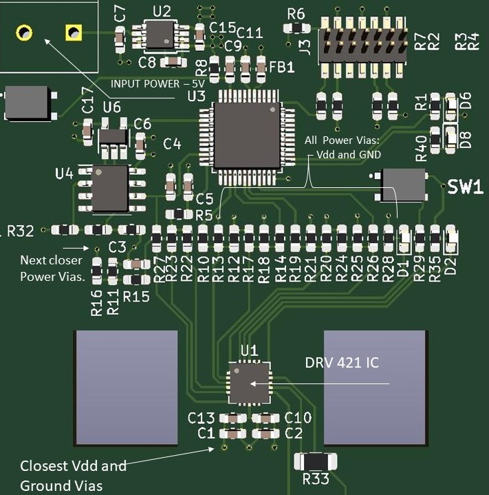
This question is related to the PCB layout for the Sensor:

4.      There are around 38 VDD (3.3 V) and Ground vias on the top layer atleast with a distance of 3  - 11 mm from the DRV421 IC. An image is shown below:


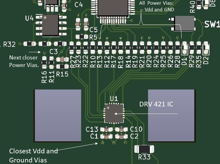
Is it advisable to keep these many vias on the same layer as the DRV 421 , it being very sensitive to stray magnetic flux ?  Also , there are Ground and Vdd (3.3 V) planes just below the top layer. Is this advisable also ? As the currents passing on the ground plane will have magnetic flux perpendicular to the DRV 421 (not along its sensitive axis) but the Vias might have flux along the sensing direction. 

Should I preferably keep the vias as far as possible from the DRV IC ? 

Note :  The PCB is around 6.8 x 6.3 cms } 

5.     Do we need an external Degauss circuit ? Or the Demag option available within the IC would be perfect ? This is just a trial but idea is to extend the range of sensing to 100 - 200 A differential currents also later.

6.    Just wished to know how the fluxgate exactly works within the sensor. Does the IC have an inbuilt PWM with Schmitt Trigger sending AC  pulsating square waveforms or it is just a pulse like a hall effect sensor ?

        Would be great to know atleast with a waveform and operation of the DRV. I have read the entire datasheet and application but the exact operation is not known to us. It would be helpful in further designs.

Atleast we would like to get the questions 1 - 3 cleared as  we need to order the core earlier.

We have more doubts on the Schematics but I will post it if it is possible for you after your reply to prevent confusion. It is quite confidential but if any other email is available to address those specific questions I can send it there.

Thanking You,

Balaji Subramanian

  • Balaji,

    There is a lot to go through here.  I will go through it an answer you later today or tomorrow.

  • Dear Mr. Javier,

    Thank you very much for replying. The first image I noticed has appeared similar to the PCB picture I have pasted at the very end. 

    This is the first image I was referring to as the design idea for the RCD:

    There 3 types of PCB used here in general.

    1.  Topmost is the Sensor PCB - PCB having the sensor and its circuitry.

    2.   The Secondary winding PCBs stacked on top of each other ( Planar winding PCBs around 6 - 9 PCBs with 218 turns on each PCB ). The above image is just for representation. The winding will be done surrounding the Left core leg.

    3.     The bottom most PCB is the Power Track PCB with the Cu traces carrying ± 10 A and 360 -  380 V DC.  Here there are just 3 tracks : +ve, -ve and Neutral Poles.  Neutral is placed on top most layer as it's Cu trace thickness is 35 µm and which is different than the inner layers. We wanted to keep the +ve and -ve traces of equal length and dimensions to correctly nullify/ negate any 'differential flux' on the DRV421 and maintain '0' during non - fault conditions.

             Aim is to sense ± 20 - 30 mA 'differential current' on the DRV 421.  

    From the simulations we could see that for 20 mA case, we are only able to obtain around 16 - 19 µT for  20 mA

    Will this sensitivity be enough for good detection or we must have atleast 200 µT for 20 mA for e.g. to have the best chance at proper and accurate detection?

    For shielding we are considering to use a Steel cube enclosing atleast a part of PCB like a cage, only allowing 2 or 5 holes for the input power. 

    The shielding has not yet been simulated but any advice for this design would be very good.

    Just wished to inform you that some part of this project is confidential hence I had opened a case with the questions in .pdf format. If possible I think it would be good if you could reply directly to my University email through there and this one in public forum can be deleted. Kindly let me know if this possible.

    Thanking You,

    Balaji Subramanian

  • Hello Balaji,

    Thanks for your questions.  I will answer based on the numbers.

    1. Here is a diagram of the location of the sensor location it is the same location as the DRV425.   The angle can vary a couple of degrees but for a close loop system this will not impact as the coupling from primary and compensating current are through the core.
    2. I cannot give that information out and and the area is small in the package that it will not disturb the field seen.  You can simulate it as a point at location mentioned above.  

    3. No the core for the compensation core should never saturate and could cause issues of getting magnetized and creating an error.

    4. When measuring low fields the current for VDD will matter but it does depend on the routing under the sensor and the current density at that point.  For example if you have a trace centered under DRV425 going right through the center this would be a greater error than a place where the current is distributed.  I think this could be an error but would likely be in the range of the offset of the flux gate.]

    5.I would use an external Degauss for two reasons.  One is that adding a larger Rshunt to get the resolution will cause limitations to drive the compensation core to a point that will be deguassed.  Second is the degauss circuit seems to have some issue with some cores.  Also I have driven and external degauss and behaves better when a current is already applied as you have to overcompensate for that current.

    6.  Here I cannot share this information.  I will need to see what is published that I can share.  I can investigate if you like but I do not expect I can share much on this front.

    Please be aware that our flux-gate offset is 8µT. 

    Other notes.  

    Coupling between compensation current and primary current ideally is matched between the two.  The locations of the sources matter as the closer current could couple to the sensor directly instead of through the core.  

    The other air gaps will reduce the coupling in the core.  Higher permeability will help but trust your simulations as they have always matched my real world.  The only time they differ is when I do not account for something.

    Shielding will be important as you at small fields could change your measurement easily.  Earths field will impact it as ~60µT and orientation is as large as your signal.  This will not be the only thing you are shielding it from.  Also think of shield as redirecting flux away, because this is what is happening.  The holes will matter.  You can easily simulate this and see the changes.  

    We can address confidential material offline.

  • Dear Mr. Javier,

    Thank you very much for answering all the questions. Now it is a bit clearer on the DRV421 operation and sensitivity.

    4. Thank you for explaining this as there are more Vdd and GND vias linking to bottom layers at many locations on the pcb top layer. 

         But there are no traces routed directly underneath the DRV421 on any layer as passing directly through the centre. I think this is what you meant would

         cause the error ?  All the tracks connect to the pins of the DRV 421. I am concerned of the vias as there might be as you explained a horizontal

          flux in direction of the line of sensitivity of the sensor. If the offsets due to the flux caused by these vias are 8 µT each, then won't it be a large offset on 

           the sensor output ? along with the internal 8 µT offset ? Or is degauss function meant to remove this internal offset after powering the sensor circuit and

           while not taking any readings ?

    May I know what probe material you would recommend if we consider using the DRV401 ? Is it required to be a saturable material or simple steel would be good ? It would actually be helpful to know this. 

    Additionally it would be great if you can investigate point 6 and answer me in the private email. I will send you the other doubts and questions via the email.

    Any of the points you cannot explain here , please let me know through email. 

    Thanking You,

    Balaji Subramanian

  • Balaji,

    I have answered in sections in your reply and changed font color.

    Balaji Subramanian1 said:

    Dear Mr. Javier,

    Thank you very much for answering all the questions. Now it is a bit clearer on the DRV421 operation and sensitivity.

    4. Thank you for explaining this as there are more Vdd and GND vias linking to bottom layers at many locations on the pcb top layer. But there are no traces routed directly underneath the DRV421 on any layer as passing directly through the centre. I think this is what you meant would cause the error ? 

    This is correct as traces/current would be the closest to the DRV421 causing a magnetic field. If the return current is in the same proximity it will cancel out.

    All the tracks connect to the pins of the DRV 421. I am concerned of the vias as there might be as you explained a horizontal flux in direction of the line of sensitivity of the sensor. If the offsets due to the flux caused by these vias are 8 µT each, then won't it be a large offset on the sensor output ? along with the internal 8 µT offset ?

    The vias are where the current can concentrate if you have planes supplying both the VDD and GND but you need to look at the distance from the sensor to see the error it can cause. If you place the GND (return current) in the same proximity they will cancel each other out when they are equal. They should be equal for the most part.

    Or is degauss function meant to remove this internal offset after powering the sensor circuit and while not taking any readings ?

    The degauss function is meant for the magnetic core but please use external as you may see issues over temperature and drive capability as normally your Rshunt will be large and not allow enough current to degauss your core.

    May I know what probe material you would recommend if we consider using the DRV401 ? Is it required to be a saturable material or simple steel would be good ? It would actually be helpful to know this. 

    The flux-gate probe requires that the probe gets saturated. Without this the principle will not work. It must saturate with the given current from IS pins and fast enough for the comparator to determine a saturation point. This is described more in detail in the DRV401 datasheet in the probe section

    Additionally it would be great if you can investigate point 6 and answer me in the private email. I will send you the other doubts and questions via the email.

    Any of the points you cannot explain here , please let me know through email. 

    Thanking You,

    Balaji Subramanian

  • Hi Mr. Javier,

    Thanks for clearing my doubts. Actually I had one more point I wished to ask in the forum:

    Is it necessary that the sensor module is designed for a sensitivity of min. 100 - 500 µT for 20 mA ?  

    In the datasheet it is written ideally ( 500 µT/A ) is preferred.

    From the simulation I made, I am getting around 1 mT for 1 A differential current between any of the three polarities. 

    But for 20 mA  we get only 15 - 19 µT 

    Is this value (15 - 19 µT ) good enough for detection purposes using DRV 421 or do you recommend that we try to have a higher flux density if possible ?

    From the datasheet I gather that ( 500 µT/ A) is for sensing 1 A differential current. Can this be taken as standard reference for Residual Current detection also ?

    I will send you the other questions.

    Thank You.

  • Balaji,

    This is not easy and you will come across even things I may not have seen.  You need to make sure increase the signal as much as you can but you will be limited by the magnetics and the mechanical placement. 

    Please make sure you have in your simulation you account for the distance the sensor is from the sensor.  The higher the signal the better but you will the 500µT/A is normally what you get with the air gap and the sensor placement.  

    This is a challenge and they signal range is near the lower range limitations of the DRV421 fluxgate.  You need to take all the drifts and changes as this is near offset.

    I do not know if the signal is large enough as I think account for so much more as the signal is in the offset range as I mentioned.

    The 500µT/A comes from the airgap and placement limitations of the sensor.

  • Dear Mr. Javier,

    Thank you very much for the reply and pardon my delay in response. I made a few simulations I had to complete to come to a conclusion.

    Can you suggest any good driver or an external degauss circuit in general for the DRV 421 Sensor ? The ones you may have used like a circuit diagram atleast how an external degauss can be implemented?

    As per my senior colleague who works in Protection says that : Since the current is controlled by the DRV421 and is determined by the 'Turns Ratio' , a driver in series would not be useful. 

    Is this correct ? 

    As per my understanding from your previous response , a driver will increase the voltage across the ICOMP terminals thereby increasing the current (V/[R_series + R_shunt] ). Is this a correct understanding of the driver function ?

    Sorry for asking any repeated questions if any. I just wished to confirm this due to the confined space we have for the driver to be placed.

    Thank you very much,

    Balaji Subramanian

  • Balaji,

    See attached.DRV421_Degauss_External_Circuit.pdf

    This is and example and how you can implement it on your own.

    I agree with you colleague as you cannot drive the same from the example I sent you there is an switch that I used.  I understand but an additional driver would increase the current.  I am not sure if we are on the same page here.  Let me know if what I sent you helps and then let me know if there is further questions.

  • Dear Mr. Javier,

    Thank you for the reply. I am working on the Degauss. There were two more questions I wished to ask you :

    1.] In the image below , I have placed the filtering capacitances C13, C10, C1, C2 very close to the sensor terminals (around 0.2 mm) which will come under the magnetic core's air gap of 0.2 - 0.3 mm. Should I place these capacitors a bit farther from the core ? How far is ideal ? Will it affect the sensing in the DRV 421 if placed very close to it's terminals? In the datasheet under "Layout Example" , the image, Capacitors are be placed very close to the sensor terminals. While it also says "Keep area free of any components creating magnetic field". 

    2.]  The Shunt resistor (Rshunt) you can see in the image above R33 is 1206, around 5 - 10 kilo ohms or lesser. Due to availability of only 0603 resistors currently with us,  can I  use two or more 0603 resistors in series to create the same amount of Vout created by the Rshunt of 1206 series ? Is it highly recommended to use 1206 resistor as shown under "Layout Example" (pg. 36) ? Due to availability reasons we are using 0603 resistor. Kindly let me know if this is a good idea.

    3.]   A small doubt regarding "Compensation Windings" around the Magnetic Core:

           We are using a 4 - Layer PCB of 0.8 mm thickness. 

            We are having 56 turns on the exterior sides and 51 - 52 turns on the Inner Layers.

            In total  -  214 - 216 compensation turns per PCB.   

            The core as I had mentioned before is a Rectangular (Racetrack Core ) and will have the planar windings on the shorter limbs.

            As per your experience, would it be good to have windings on "Both the Core limbs" meaning Split the windings per layer on two core limbs ?  

           I currently have a planar winding only around one limb.

           Will this help reduce any leakage flux and provide better compensation ?

            The operation is in Pure DC and will not have AC of any kind.  Is winding around both cores advisable in this case ?

    4.]     Sir, I just wish to know what is the exact relation between "Higher Flux Density" on DRV 421 and the Output Vout ?

             Will higher flux density only increase the voltage across the windings for better driving capability ?

              Because currently we are able to obtain around 69 - 78 uT  by considering that the "Probe" inside the DRV is iron having relative permeability = 100.

              Kindly advise on this.

              Since the sensor needs to be precise and accurate, I am very worried that the results will have a lot of errors.

              This is the reason I requested for the inner operation and any info. on core inside the DRV 421.  Please advise on the relation between the flux density

               and output. Any example with explanation would do as well.

              We wish to have lesser than 0.1 % error since this device is to be used for detection residual currents. This is the concern.

    Thank you very much Mr. Javier, awaiting your reply. Would be nice to receive it today as we plan to order my PCB today.

    Balaji Subramanian

  • Balaji,

    Javier unfortunately is out today on holiday. I have notified him of the additional information you've provided, and he will reply with comments Monday morning when he returns to the office. 

  • Dear Mr. Andrews,

    Thank you very much for replying to my question. It is not a problem at all, we have delayed the ordering of the PCB until 19th  Monday to get clarity on how our design will impact the sensing.

    It would be very helpful to receive Mr. Javier's views on the questions. We are developing a Residual Current Detector to detect very small currents in the range of 20 - 30 mA across a voltage of ± 380 V DC (pure DC).

    We work on DC Microgrids and upcoming future technologies for independent meshed grids. In DC we are using a special grounding system which makes differentiation between small currents and large ones hard.

    Main reason why we need the  < 0.1% accuracy in our readings. Of course many factors depend upon the physical constraints of the device, some advice on how the flux density on the fluxgate sensor directly

    impacts the Vout being sensed, would be very helpful to know.

    Like if the high Flux ( 500 uT / A) as specified in the datasheet, determines the Voltage which will drive a compensation current  ? Meaning at DC , the current compensation is directly decided by the fluxgate potential

    or the sensor just acts like a switch - closing the compensation circuit to obtain zero flux in the core ? This is my most fundamental doubt. 

    I have also sent an email to Mr. Javier regarding a few design issues which are confidential.

    Thanking You,

    Balaji.

  • Hello Balaji,

    Here is my reply from the previous questions.  Thanks for being patient.  I will look at your confidential material you sent through email.  

    1]

    There are capacitors that have non-magnetic materials. These are the ones that should be used. Please be aware some capacitors state they have non-magnetic materials but after evaluating them I have seen they actually do have material that does have material that has some permeability. If you use some of the capacitors without magnetic material your placement is fine. If you cannot I would move capacitors lower and below the core.

    Also please separate capacitors connection like seen on figure 71 in the datasheet for the capacitors. You should have for example C13, C1 connected to pin 8 and C10,C2 connected to pin 9.

    2]

    The size of the resistor is more due to power constraints. The main design for the DRV421 is for larger currents so the 1206 resistor could matter. The size or resistor is only due to power. With large resistor you could worry about stability. Depending on the inductance and your Rshunt you could have issues. See this application note.

    3]

    From my experience symmetrical is always best. So a core with windings distributed over the whole core windings are better than if the compensation windings were on only one side. Think of this a magnetic coupling. The higher the permeability of you core the less of an issue as all the magnetic coupling happens in the core and the flux does not escape the core. This could be simulated by getting the entire mechanical placement in place and look at the simulation, but the easiest way to approach is to have it symmetrical. Your air gaps I believe will be your biggest issues as these will be hard to control.

    You want to make sure you windings don’t couple magnetically directly to your sensor but couple to your core. This is done by having compensation windings closer to your core and further from the DRV421 sensor. You want all magnetic coupling happening through the core.

    Same as above you want couple through the core. Place an AC filter to the lowest frequency response you can accept. This will reduce some noise.

    4]

    The easiest way to explain this is the DRV421 is pushing current on the compensation winding to place 0 field at the sensor inside the DRV421. There is an offset so you need to take that into account.   As the field increases the DRV421 drives form current on the compensation windings to balance it to zero. Therefore you will have more current on your Rshunt increasing your voltage. The higher the flux density you could think of it as your signal. So having the highest magnetic gain is best.

    This is signal to noise that is going to be an issue. As we go down in signal our noise/offset plays a larger role in our error.

    I cannot give the internal properties of the probe information.

    Like I mentioned before I think this is very difficult to do with the mechanical limitations and magnetic coupling.  0.1% at such a low signal level relative to the offset and noise.  With a core of 500µT/A the offset is 16mA from the offset of 8µT.  You can see that the offset a large part of the error and even if you eliminate the offset the drift, noise, and other changes from ideal near the offset are going to be issues.  Because the sensor cannot get placed closer to the air gap of the core you cannot get much more flux at the sensor and cannot increase the gain much more than the 500µT/A.