


Hello,
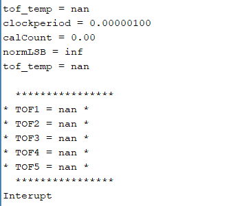
I have a problem with the following arduino-program for the TDC7200. My problem is that I don´t get values for the CALIBRATION1 and CALIBRATION2, therefore the serial monitor gives following out: (picture) Maybe anyone can fix the problem!
Parts of the program are from: github.com/.../TDC7200
Header-Program:
#ifndef TDC7200_H
#define TDC7200_H
int csPin = 53;
// parts of this code taken from github.com/.../TICC
#define SPIfrequency (uint32_t) 2500000
#define EXTCLOCK (uint32_t) 1000000 //Value of external CLOCK for 1MHz
#define AVG_CYCLES 10
// TDC7200 register addresses
const int CONFIG1 = 0x00; // default 0x00
const int CONFIG2 = 0x01; // default 0x40
const int INT_STATUS = 0x02; // default 0x00
const int INT_MASK = 0x03; // default 0x07
const int COARSE_CNTR_OVF_H = 0x04; // default 0xff
const int COARSE_CNTR_OVF_L = 0x05; // default 0xff
const int CLOCK_CNTR_OVF_H = 0x06; // default 0xff
const int CLOCK_CNTR_OVF_L = 0x07; // default 0xff
const int CLOCK_CNTR_STOP_MASK_H = 0x08; // default 0x00
const int CLOCK_CNTR_STOP_MASK_L = 0x09; // default 0x00
// gap from 0x0A thru 0x0F...
const int TIME1 = 0x10; // default 0x00_0000
const int CLOCK_COUNT1 = 0x11; // default 0x00_0000
const int TIME2 = 0x12; // default 0x00_0000
const int CLOCK_COUNT2 = 0x13; // default 0x00_0000
const int TIME3 = 0x14; // default 0x00_0000
const int CLOCK_COUNT3 = 0x15; // default 0x00_0000
const int TIME4 = 0x16; // default 0x00_0000
const int CLOCK_COUNT4 = 0x17; // default 0x00_0000
const int TIME5 = 0x18; // default 0x00_0000
const int CLOCK_COUNT5 = 0x19; // default 0x00_0000
const int TIME6 = 0x1A; // default 0x00_0000
const int CALIBRATION1 = 0x1B; // default 0x00_0000
const int CALIBRATION2 = 0x1C; // default 0x00_0000
class tdc7200 {
private:
float clockperiod = 1.0 / EXTCLOCK;
public:
uint32_t time1 = 0;
uint32_t time2 = 0;
uint32_t time3 = 0;
uint32_t time4 = 0;
uint32_t time5 = 0;
uint32_t time6 = 0;
uint32_t clockcount1 = 0;
uint32_t clockcount2 = 0;
uint32_t clockcount3 = 0;
uint32_t clockcount4 = 0;
uint32_t clockcount5 = 0;
uint32_t cal1 = 0;
uint32_t cal2 = 0;
float tof1 = 0;
float tof2 = 0;
float tof3 = 0;
float tof4 = 0;
float tof5 = 0;
//READ 8bit Register
byte readReg8(byte address) {
byte inByte = 0;
digitalWrite(csPin, LOW);
SPI.beginTransaction(SPISettings(SPIfrequency, MSBFIRST, SPI_MODE0));
// take the chip select low to select the device:
SPI.transfer(address & 0x1f);
inByte = SPI.transfer(address);
digitalWrite(csPin, HIGH);
SPI.endTransaction();
return inByte;
}
//READ 24bit Register
uint32_t readReg24(byte address) {
long value = 0;
// CSB needs to be toggled between 24-bit register reads
SPI.beginTransaction(SPISettings(SPIfrequency, MSBFIRST, SPI_MODE0)); // SPI Einstellungen setzen
digitalWrite(csPin, LOW);
SPI.transfer(address & 0x1f); //Hintersten 5 BIT werden angeschaut
long msb = SPI.transfer(address); // Ersten 8 Bit
long mid = SPI.transfer(address); // Mittleren 8 Bit
long lsb = SPI.transfer(address); // Letzten/Niederwertigsten
value = (msb << 16) + (mid << 8) + lsb;
SPI.endTransaction();
delayMicroseconds(5);
digitalWrite(csPin, HIGH);
return value;
}
//WRITE REGISTER
void writeReg(byte address, byte value) {
uint16_t test = 0;
// take the chip select low to select the device:
SPI.beginTransaction(SPISettings(SPIfrequency, MSBFIRST, SPI_MODE0));
digitalWrite(csPin, LOW);
// Force Address bit 6 to one for a write
SPI.transfer16((address | 0x40) << 8 | value);
test = (address | 0x40) << 8 | value;
Serial.print("-----test = "); Serial.println(test, BIN);
digitalWrite(csPin, HIGH);
SPI.endTransaction();
}
//COMPUTE TOFs
float getTOF(uint32_t timeN, uint32_t timeN1, uint32_t clockcountN, uint32_t cal1, uint32_t cal2) { // uint_32 = unsigned int
float calCount = (cal2 - cal1) / (AVG_CYCLES - 1.0);
Serial.print("clockperiod = "); Serial.println(clockperiod,8);
Serial.print("calCount = "); Serial.println(calCount);
float normLSB = (clockperiod / calCount);
Serial.print("normLSB = "); Serial.println(normLSB,8);
float fehler = timeN-timeN1;
float tof_temp = normLSB * (float(timeN) - (float)timeN1) + clockcountN * clockperiod;
// float tof_temp = (float timeN)* normLSB + clock_countN*clockperiod;
Serial.print("tof_temp = "); Serial.println(tof_temp, 16);
return tof_temp;
}
};
#endif /* TDC7200_H */
Arduino-Program:
#include <SPI.h>
#include "tdc7200.h"
int startpin = 4;
int stoppin = 7;
int triggerpin = 8;
int enable = 3;
int intb = 2;
const byte CLOCKOUT = 11; //CLOCK ON MEGA2560
byte config1, config2, int_status;
byte int_mask, ccoh, ccol, clockcoh, clockcol, clockcstopmaskh, clockcstopmaskl;
void setup() {
// Initialize 1 MHz clock on CLOCKOUT (OC1A)
pinMode (CLOCKOUT, OUTPUT);
// set up Timer 1
TCCR1A = bit (COM1A0); // toggle OC1A on Compare Match
TCCR1B = bit (WGM12) | bit (CS10); // CTC, no prescaling
OCR1A = 7; // output every cycle
//Initialize SPI
SPI.begin(); //chip1Select = 53
//Initialize Serial
Serial.begin(19200);
//set cs pin output
pinMode(csPin, OUTPUT);
//Initialize Outputs
pinMode(enable, OUTPUT);
//digitalWrite(enable, LOW);
pinMode(startpin, OUTPUT);
digitalWrite(startpin, LOW);
pinMode(stoppin, OUTPUT);
digitalWrite(stoppin, LOW);
//Initialize INPUTS
pinMode(intb, INPUT);
pinMode(triggerpin, INPUT);
//STARTUP OF TDC7200
digitalWrite(enable, LOW);
delay(2);
digitalWrite(enable, HIGH);
delay(2);
}
void loop() {
tdc7200 chip1;
digitalWrite(enable, LOW);
//WRITE 00000011 INTO CONFIG 1 TO GET READY FOR MEASUREMENT1
chip1.writeReg(CONFIG1, B00000011);
//WRITE B01000011 INTO CONFIG2 for FOUR STOPS
// 000: Single Stop
// 001: Two Stops
// 010: Three Stops
// 011: Four Stops
// 100: Five Stops
chip1.writeReg(CONFIG2, B01000100);
//READ IF CONFIG1/2 CORRECT
config1 = chip1.readReg8(CONFIG1);
config2 = chip1.readReg8(CONFIG2);
//WAIT for Trigger Signal == 1
//while(digitalRead(triggerpin));
//SEND START
digitalWrite(startpin, HIGH);
digitalWrite(startpin, LOW);
delayMicroseconds(100);
//SEND 5 STOPS
for (int i = 0; i <= 4; i++) {
digitalWrite(stoppin, HIGH);
digitalWrite(stoppin, LOW);
delayMicroseconds(100);
}
//READ REGISTERS AND COMPUTE VALUES
chip1.time1 = chip1.readReg24(TIME1);
chip1.time2 = chip1.readReg24(TIME2);
chip1.time3 = chip1.readReg24(TIME3);
chip1.time4 = chip1.readReg24(TIME4);
chip1.time5 = chip1.readReg24(TIME5);
chip1.time6 = chip1.readReg24(TIME6);
chip1.clockcount1 = chip1.readReg24(CLOCK_COUNT1);
chip1.clockcount2 = chip1.readReg24(CLOCK_COUNT2);
chip1.clockcount3 = chip1.readReg24(CLOCK_COUNT3);
chip1.clockcount4 = chip1.readReg24(CLOCK_COUNT4);
chip1.clockcount5 = chip1.readReg24(CLOCK_COUNT5);
chip1.cal1 = chip1.readReg24(CALIBRATION1);
chip1.cal2 = chip1.readReg24(CALIBRATION2);
Serial.print("--- cal values: ");
Serial.print(chip1.cal1);
Serial.print(", ");
Serial.println(chip1.cal2);
//END OF READ REGISTERS
chip1.tof1 = chip1.getTOF(chip1.time1, chip1.time2, chip1.clockcount1, chip1.cal1, chip1.cal2);
chip1.tof2 = chip1.getTOF(chip1.time1, chip1.time3, chip1.clockcount2, chip1.cal1, chip1.cal2);
chip1.tof3 = chip1.getTOF(chip1.time1, chip1.time4, chip1.clockcount3, chip1.cal1, chip1.cal2);
chip1.tof4 = chip1.getTOF(chip1.time1, chip1.time5, chip1.clockcount4, chip1.cal1, chip1.cal2);
chip1.tof5 = chip1.getTOF(chip1.time5, chip1.time6, chip1.clockcount5, chip1.cal1, chip1.cal2);
//TESTPRINT CONFIG1/2
//Serial.print("CONFIG1 = "); Serial.println(config1, BIN);
//Serial.print("CONFIG2 = "); Serial.println(config2, BIN);
Serial.println();
Serial.print(" ****************");
Serial.println();
Serial.print("* TOF1 = ");
Serial.print(chip1.tof1, 8); Serial.println(" *");
Serial.print("* TOF2 = ");
Serial.print(chip1.tof2, 8); Serial.println(" *");
Serial.print("* TOF3 = ");
Serial.print(chip1.tof3, 8); Serial.println(" *");
Serial.print("* TOF4 = ");
Serial.print(chip1.tof4, 8); Serial.println(" *");
Serial.print("* TOF5 = ");
Serial.print(chip1.tof5, 8); Serial.println(" *");
Serial.print(" ****************");
Serial.println();
if (digitalRead(2)) {
Serial.println("Interupt");
}

