Other Parts Discussed in Thread: PGA460
PGA460-Q1 Two-Wire Ultrasonic Sensor Module (TWSM)
The PGA460Q1TWSM is a variant of the PGA460-Q1 small form factor reference design for systems which require a two-wire ultrasonic sensor module solution, whereby one-wire interface data is transmitted over power. This module only requires VPWR_IO and GND pins. Here is the PGA460Q1TWSM schematic:
where the add-on components from the original small form factor solution required enable the two-wire interface are as follows:
-
- R2 = serial current-limiting supply resistor (alternative can be an inductor for EMC purposes)
- D1 = reverse polarity protection diode
- C5 = reservoir capacitor for VPWR (prevents under-voltage condition)
- C6 = blocking supply capacitor (optional)
- R6 = serial resistance for IO line (optional; placeholder for additional resistance or inductance)
- C14 = capacitor for IO line (optional)
In this schematic, two electrolytic capacitors are present. If the system does not require R1 (serial resistor for transformer’s center-tap), then a single electrolytic can be shared by both VPWR to save on components-count and cost. However, the TWSM then relies on R2 to limit the in-rush current to the center-tap's charge capacitor, which may cause VPWR to droop during burst.
For automotive demonstration purposes, the PGA460-Q1 EVM’s IO pin at J6-2 is used to emulate a Body Control Unit (BCU) VPWR_IO connection. The user is required to desolder the EVM's shunt at R15 to prevent TCI/OWU communication with the PGA460 IC on-board the EVM. Also, reducing the EVM’s IO pull-up at R20 from 1kOhm to 0.1kOhm is required to allow a sufficient amount of current to supply the TWSM.
PGA460-Q1 EVM modifications:
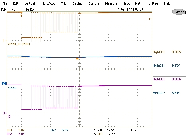
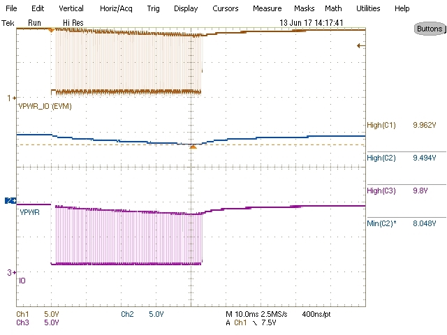
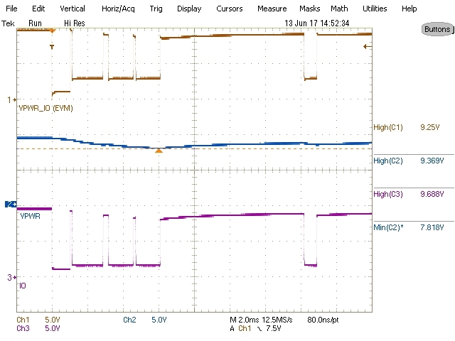
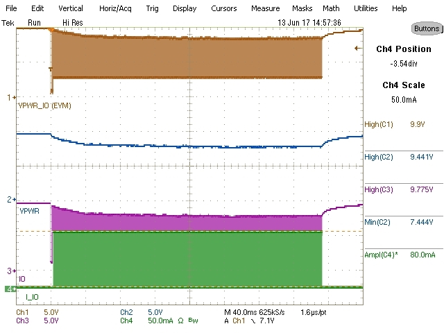
After applying the aforementioned modifications to the EVM, and connecting the TWSM to the EVM, the example TCI results are as follows:
Due to the two forward voltage diode drops from the EVM’s D11 and the two-wire module’s D1, and the current limited IO master on the EVM, the static supply voltage is not 12V as sourced from the main PSU, but at 9~10V at VPWR of the TWSM. Depending on how the customer intends to test the TWSM (i.e. with an actual BCU), the amount of voltage drop can be reduced/controlled.
The GUI can be used to read and write the TWSM’s registers exclusively through the Interface Mode --> IO TCI page. Here I was able to confirm that the oscilloscope activity matched the GUI display:
TI will continue to optimize and simplify the schematic, but the presented means of experimentation is a proven starting point to for any interested user.


