


The Autonomous Audio Accessory and Switch Routing IC line from Texas Instruments includes the TS3A225E, TS3A226AE, and TS3A227E devices. At first glance these parts can seem difficult to integrate into the system in the most optimal way – this FAQ will quickly walk through how to design this line of parts into your system.
To simplify the devices the pins can be categorized into five general groups:
- Power
- Communication
- Detection
- Switch connection + Measurement
- /MIC_PRESENT (TS3A227E and TS3A225E only)
POWER PINS
The first pin group is the power pin group, which will include power and ground connections for the devices. As with most IC’s, supply decoupling capacitors are recommended. For these devices two are recommended, one 1uF and one 0.1uF recommended. For VDD layout keep the capacitors as close to the pin as possible. As for Ground pins the devices have a bit of a deviation as they include different references for different ground connections.
- TS3A225E Ground Connections:
- GND -> Connect all GND pins to System Ground
For the 225E the ground connections act as the ground of the system and connecting them all to ground is an acceptable move.
- TS3A226AE Ground Connections:
- GND -> Connect to System Ground
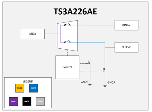
- GNDA -> GND Reference for FET1
- GNDB -> GND Reference for FET2
For the 226AE the ground bus is separated into three different sections. The system ground can be connected to all three of these points for simplicity. However, if an FM ground network is needed the FM matching network can be connected to GNDA and GNDB pins with GNDA and GNDB shorted together.
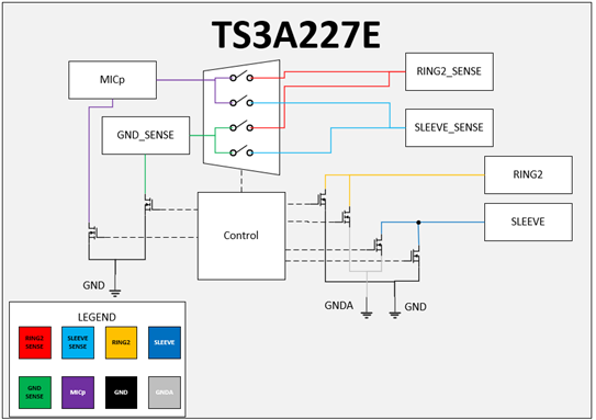
- TS3A227E Ground Connections:
- GND -> Connect to System Ground
- GNDA -> Equivalent to GNDA + GNDB in 226AE
- GND_SENSE -> Codec Ground Reference
The 227E has three ground pins as well. The first is the system ground which is the same as the other two devices. GNDA is the depletion FETs reference point – if using a FM matching network use GNDA to connect the FM matching circuit. If not using a FM matching network connect GNDA to GND. GND_SENSE is should be tied to the Codec’s ground – which in many applications is also the system ground.
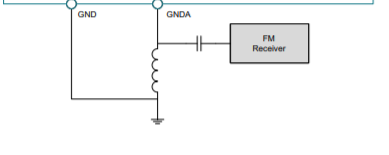
FM support is also possible through these devices by using the separate ground pins. To support FM transmission, connect the ground reference pins to the system specific matching network to support FM transmission for mobile audio applications. Below is an example of the FM matching network on the 227E – however the same idea can be applied to the other devices.
COMMUNICATION
On these devices only the TS3A225E and TS3A227E support communication. The communication protocol used for both devices is I2C. These pins are optional as there are default settings that may not need to be changed through software. Both the 225E and 227E both have an SDA line and a SCL line. A pull-up resistor should be used if these pins are active; however, if these pins will not be used these pins can be directly connected to VDD.
The TS3A225E has a I2C address select pin, this allows the device to choose its address with a low signal generating a write address of 8’h76 and read address of 8’h77 while a high signal has a write address of 8’h78 and a read address of 8’h79. If this pin is unused it should be connected to ground. The TS3A227E does not support this feature and only includes one I2C address which is 8’h76 for write and 8’h77 for read.
The TS3A227E has an /INT pin for an interrupt flags thrown during I2C communication. If used, use a pull-up resistor to tie to I2C voltage supply as this is an open drain output. If unused this pin can be grounded. The T3A225E does not support the /INT pin and if this is required the TS3A227E is the correct device.
DETECTION
The detection pin on the device is the input for the signal that triggers the device to detect impedance and route the accessory based on what type is detected. This section only deals with hardware generated detection instead of software generated detection which can be triggered on the 225E and 227E. All three devices have one detection input pin, when a signal transition is measured on this pin there will be a delay and then the detection algorithm will run. Depending on the exact part used this pin acts a bit differently.
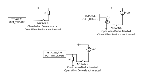
For the TS3A225E, the detection pin is labeled DET_TRIGGER. When a low to high transition is registered on this pin the delay + detection sequence will start (for more information on detection please see our FAQ on the subject here). When a high to low transition is seen the device will detect an accessory removal.
The TS3A226AE is very similar to the TS3A225E – the only difference is that the detection pin is labeled as EN, but it acts in the same way.
The TS3A227E has its detection pin labeled as /DET_TRIGGER. There are two differences on this pin. The first is that the device is looking for a high to low transition as opposed to the 226AE and 225E which are looking for low to high transitions for insertion detection. Secondly, this pin is internally pulled up to VDD so no external pull-up resistors are needed to keep this high during times when an accessory is not inserted.
The most common connection for this pin on all the devices is to have it connected to the audio jack so that insertions and removals of the accessory trigger voltage transitions. This is since many 3.5mm jacks include either pins that are shorted together until a device is inserted (NC) or pins are open circuited until a device is inserted (NO).
The accessory jack in this scenario includes a mechanical switch that can physically bounce upon contact causing noisy signals on the detection pin, but utilizing the internal debounce delay, and possibly the addition of external RC components, false detections can be mitigated. Another benefit is that on the 225E and 227E these delays can be lengthened in software to up to 2 seconds to help mitigate issues of incorrect detection accessory due to slow insertion.
SWITCH CONNECTION + MEASUREMENT
The next category deals with all the connections that are used to route audio signals between their inputs and outputs. This includes the 3.5mm jack connections as well as the connections to the Audio Codec.
All three devices contain the following pins TIP (TIP_SENSE in TS3A227E), RING2, SLEEVE, and MICp. The TS3A225E and TS3A227E also have a connection to the GND of the Codec called MICn and GND_SENSE respectively. For the 3.5mm jack connections (TIP, RING2, and SLEEVE) – these pins should be connected directly to the 3.5mm jack. These traces should be low impedance and short, as in that the IC should be place as close as possible to the audio jack. The TIP pin can be thought of as a positive terminal of an Ohmmeter where the negative terminals are on the RING2 and SLEEVE connections of the IC.
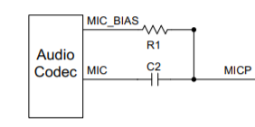
The RING2 and SLEEVE pins in all the devices are connected to FETs that can ground either RING2 or SLEEVE depending on what type of accessory is detected. In the TS3A226AE the RING2 and SLEEVE pins are also used to route the signals to the microphone and Codec reference. MICp is present in all three IC’s and is the connection point to the Audio Codec. If a microphone is detected, which means a 4-pole device was detected, this pin will route either SLEEVE or RING2 signals to the Codec. This pin typically has the MICp signal as well as a microphone bias – a quick example is shown below and components will depend on Codec and application.
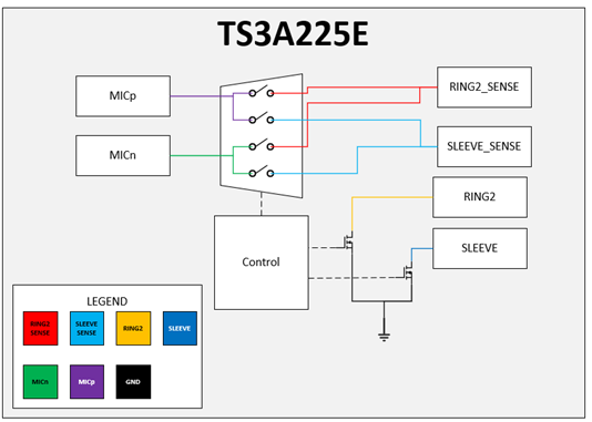
The TS3A225E and TS3A227E also have a few other switch connection pins that are used. Both devices contain the following pins: SLEEVE_SENSE, RING2_SENSE, and GND_SENSE (227E)/MICn (225E). Both MICn and GND_SENSE have the same function. SLEEVE_SENSE and the RING2_SENSE pins are used to route signals from a 3.5mm accessory to the MICp and GND_SENSE/MICn as well as aid in impedance measurements during detection. SLEEVE_SENSE and RING2_SENSE should be connected directly to the 3.5mm accessory jack. GND_SENSE/MICn should be connected to the ground of the Codec, which in many cases is the system ground. Routing diagrams for the devices are shown below.
/MIC_PRESENT
The TS3A226AE pins have all been described – but the TS3A225E and TS3A227E both have one more pin that doesn’t neatly fit into the other categories. This is the /MIC_PRESENT pin. It is an open drain output – so if you wish to use this pin a pull-up resistor needs to be used – using the same ones as used in the I2C communication should be fine. This pin will go low when a 4-pole device is detected on both the TS3A225E and TS3A227E.
LAYOUT TIPS
Even with all schematic rules followed properly the layout of the subsystem is crucial for success of the application. In this line of parts there are two main groups pins which layout is very important and should take very high priority in routing the system and pins that are less burdensome.
The pins that need to be paid most attention to are the detection and switch connection pins. This group essentially is going to mainly focus on the 3.5mm jack connections and the detection trigger pin. The most important rule is that long traces a bad for these parts – and due to this the IC should be placed as close as possible to the audio jack for best results. The 3.5mm jack connections (TIP, RING2 and SLEEVE) should have the following goals met: resistance to the jack of no more than 50mΩ, placed on the same layer as the audio jack, i.e. vias are not recommended for these pins, and that I2C communication lines are routed away from these pins. The SENSE pins follow a similar rule set except that the resistance to the jack can be up to 1Ω recommended. If these pins aren’t routed with high priority the chance of needing to debug and redo the layout goes up very fast as improper layout can cause detection issues.
The other pin that layout should be paid attention to is the trigger to activate detection. The layout can affect how long the debounce period needs to be. While this can be adjusted via software in the 227E and 225E to help mitigate problems due to layout, but the 226AE does not have this feature so external RC components may need to be used, and if used they should be placed close to the trigger.
The other pins that are left have less difficult routing as they are standard I2C buses and should follow I2C bus regulations – essentially keeping low bus capacitance. The routing to the Audio Codec is typically just a straight short bus to the Codec. GND and VDD traces should be short and wide with power supply decoupling capacitors as close to the power pin as possible.