


What is Injection Current?
Injection current is the current that is being forced into a pin by an input voltage (VIN) higher than the positive supply (VDD + ∆V) or lower than the ground reference (VSS or GND). The current flows through the input protection diodes into either supply of the device potentially compromising the accuracy and reliability of the system. Injected currents can come from various sources depending on the application. Some examples of possible sources are described below:
- Harsh environments and applications with long cabling, such as in factory automation and automotive systems, may be susceptible to injected currents from switching or transient events.
- Other self-contained systems can also be subject to injected current if the input signal is coming from various sensors or current sources.
How Can This Affect Your System?
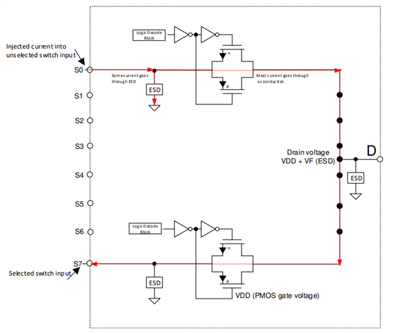
Typical CMOS switches have ESD protection diodes on the inputs and outputs. These diodes not only serve as ESD protection, but also provide a voltage clamp to prevent the inputs or outputs going above VDD or below GND/VSS. When current is injected into the pin of a disabled signal path, a small amount of current goes through the ESD diode, but most of the current goes through conduction to the Drain. If the forward diode voltage of the ESD diode (VF) is greater than the PMOS threshold voltage (VT), the PMOS of all OFF switches turns ON and there would be undesirable subthreshold leakage between the source and the drain that can lift the OFF source pins up. Below shows a simplified diagram of typical CMOS switch and associated injected current path:
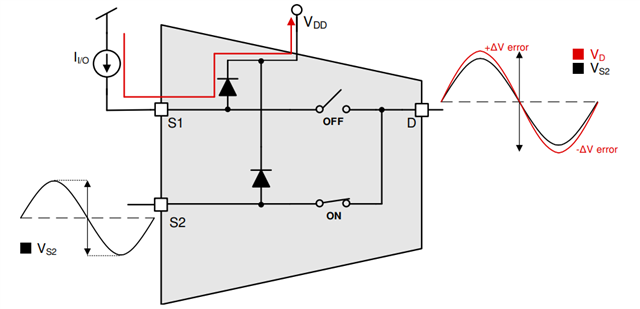
In addition, this phenomenon can also affect the ON-resistance parameter. Because the ON-resistance of the enabled FET switch is impacted by the change in the supply rail, when the drain pin voltage exceeds the supply voltage by more than a VT, an error in the output signal voltage can be expected. This undesired change in the output can cause issues related to false trigger events and incorrect measurement readings, potentially compromising the accuracy and reliability of the system. As shown below, S2 is the enabled signal path that is conducting a signal from S2 pin to D pin. Since there is an injected current at the disabled S1 pin, the voltage at that pin increases above the supply voltage and the ESD protection diode is forward biased, shifting the power supply rail. This shift in supply voltage alters the RON of the internal FET switches, causing a ∆V error on the output at the D pin.
Injection Current Control in TI Multiplexers and Signal Switches
Now that it is evident that injection current can produce some undesirable system impacts, what can be done about this? Several TI multiplexers and signal switches offer a feature called “Injection Current Control” which helps combat the effects of this phenomenon on your system. To avoid the complications of added external protection to your system, these Injection Current Control enabled devices have internal circuity which eliminates the need for external diode/resistor networks typically used to protect the switch and keep the input signals within the supply voltage. The internal injection current control circuitry allows signals on disabled signal paths to exceed the supply voltage (but not the absolute maximum voltage as specified) without affecting the signal of the enabled signal path.
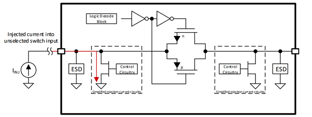
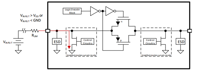
The injection current control circuitry is independently controlled for each source or drain pin (Sx, D). The control circuitry for a particular pin is enabled when that input is disabled by the logic pins and the injected current causes the voltage at the pin to be above VDD or below GND. The injection current circuit includes a FET to shunt undesired current to GND in the case of overvoltage or injected current events. Each injection current circuit rating can be found in the datasheet. Depending on the system application, a series limiting resistor may be needed and must be sized appropriately if there is a chance of exceeding this specification (note that this resistor will be required if the input signal exceeds the absolute maximum/minimum VDD/VSS-GND voltage or the injection current circuit rating):
Quantifying Injection Current Effects
Lastly, the effects of Injection Current often are shown as fluctuations in the output voltage. In some of our datasheets, we quantify how much the shift in output voltage will be affected if there is an injection event:
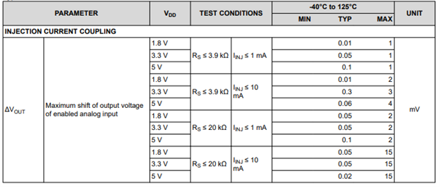
As shown in the table above, the coupling effect is proportional to the amount of current injected into the input. By limiting this current, the effects can be mitigated.
For more information on this topic, please follow the link to the video below: