This thread has been locked.

If you have a related question, please click the "Ask a related question" button in the top right corner. The newly created question will be automatically linked to this question.

TS3A24159: Correct Pin A1 Location on Component

Part Number: TS3A24159

Hello,

I have a question regarding the TS3A24159YZPR pin A1 location. It seems there is conflicting information about this in the part datasheet:

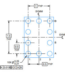
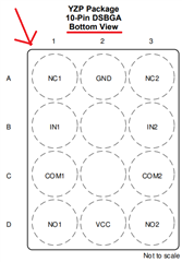
On one hand, at page 4, there is a "Bottom View" where pin A1 is shown to be in the upper-left of the component. This means that in Top View, pin A1 would be in the upper-right of the component.

On the other hand:

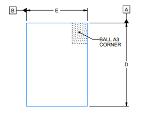
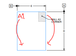
  • At page 33, in the first drawing (which seems to be a Top View, even though it is not mentioned) pin A3 is shown to be in the upper-right. This means pin A1 would be in the upper-left.
  • Also at page 33, in the second drawing (which seems to be a Bottom View, even though it is not mentioned) pin A1 is in the lower-left. This means that in Top View, A1 would be in the upper-left.
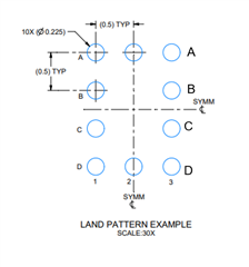
  • At page 34, in the Land Pattern Example (which I assume is a Top View), pin A1 is in the upper-left.
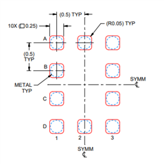
  • At page 35, in the Solder Paste Example (which I assume is a Top View too) pin A1 is again in the upper-left.
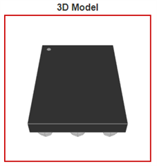
  • In the component 3D model from ultralibrarian.com, pin A1 is marked in the upper-left of the component.

So, where is pin A1 actually in the Top View of the component? In the upper-right or in the upper-left of the component?

Thank you!

  • Hey Ioan,

    There isn't a discrepancy here. A1 is in the top right corner from the top view. The device is being flipped from top to bottom to get the bottom view on page 33.


    When soldered down you'll of course want the pinout to align with how it would look from the top view though, so the land pattern and solder paste needs to align with top view pin locations.


    Thanks!
    Rami

  • Hello,

    You mentioned that A1 is in the top right corner from the top view. However, in the first drawing you attached (which should show the top view, before the component is flipped over), A1 is in the top left corner:

    Also, in the page 4 of the datasheet, there is a bottom view drawing which shows pin A1 being in the top-left corner. This would mean that in a Top View drawing, A1 would be in the top-right corner:


    Which of these two drawings is correct?

    Thank you,

    Ioan.

  • Hey Ioan,

    Sorry about that typo. Yes, I meant to say Top left from top view; where I had it drawn. 
    I see what you're seeing and I understand the confusion here. The physical indicator on the device itself will reference you to A3. However, there shouldn't be too much of a problem here either way when designing since the device itself is symmetrical. All the '1' sided signals will be on one side of the device while the 2's will be on the other. Since they have their own control INx pin, the numbering is more arbitrary and can call either side '1' or '2'. So as long as you have row A where row A should be, you should be fine. 

    Thanks,
    Rami

  • Hi Rami,

    So A1 should be in the top-left in the Top View. So all the drawings from pages 33-35 are correct.

    This means that the drawing from page 4 should be corrected, right? It is not Bottom View, it is Transparent Top View:

    Also, the 3D model from ultralibrarian.com should be corrected; in it, pin A1 is marked, when pin A3 should be marked instead:

    You are right that the IC is symmetrical by its GND-VCC axis, and the location of pin A1 should not affect the PCBs using it. However, I would like to make sure that we have the correct footprint, in case we use it for another IC in the future.

    Thank you,

    Ioan.

  • Hey Ioan,

    Yes, the drawings from 33-35 are correct.

    It does look like a transparent top view but I can't confirm anything about what the intent of the drawing was since this datasheet was created a while back so the person who initially created this is no longer on the team. But as I mentioned, it shouldn't make a difference with regards to the PCB or even if you replace it with another IC in the future. The naming convention doesn't change the functionality. So in the future, there shouldn't be any problems here. That's to say, if in a future chip we change the name of Vcc to VDD instead or IN1 to IN0, it shouldn't have an impact on how you use it or your ability to replace it since these are just nomenclatures and the physical layout is still tied together and the same.

    That being said, I understand the confusion this adds when you're trying to work with this part. I'll add this to our backlog of changes needed to be made.

    Thanks,
    Rami 

  • Hi Rami,

    Thank you for your answer!

    I understand that the respective IC has its pinout symmetrical (i.e. the left side pinout is identical to the right side pinout), and that the left side of the IC refers to one independent switch, while its right side refers to another independent switch. Thus, if we mirror the pinout by the GND-VCC axis, the design using the IC would still work fine. In that respect, the problems I mentioned above are relatively minor.

    I now corrected our footprint based on the information you wrote, and this should also help in manufacturing (i.e. correctly identifying component orientation).

    I think my issue is now resolved.

    Best Regards,

    Ioan.