


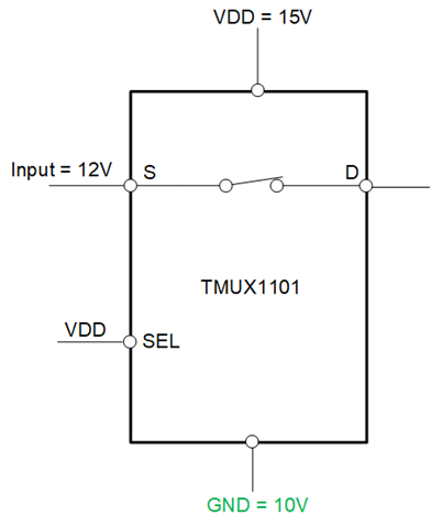
There are often systems that utilize TI Switches/Multiplexers where traditional and common supply rails are not accessible, but the designer still needs to power these devices. Fortunately, TI Switches/Multiplexers allow for ground shifting which offers great flexibility when trying to design a practical power scheme. Ground shifting can be defined as setting the ground reference on a device as a non-zero voltage which changes the operating point of the device itself. An example is portrayed below where a traditional 5V multiplexer (the TMUX1101 for instance) is powered by a 15V supply rail and a 10V supply rail connected to the GND pin. This effectively is still a 5V differential and the device will not be damaged at these voltages:
While this can come in handy when there are not many options to power such a device, there are several caveats that need to be taken into consideration. The first being the input high and input low logic control voltages (VIH/VIL). Staying with the TMUX1101 example, the below outlines the recommended operating conditions for the device and VIH/VIL levels needed for proper logic changes:


Under normal operating conditions at 5V, the TMUX1101 needs to see at least 1.49V to register as a logic high and 0.87V or lower to register as a logic low. Now with the ground shifted device above, these conditions change to the device needing to see 1.49V + VGND_Shift which is equal to 1.49V + 10V, resulting in a VIH level of 11.49V (similarly, VIL needs to be 10.87V or below). This can be particularly problematic if the address or logic pins are being connected to an MCU where that type of voltage will most likely not be available to switch with. In addition, these Switches/Multiplexers can also have a negative reference voltage as well. For clarity, see below as an example:
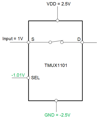
Again, the voltage differential is within specification (5V) and will be perfectly acceptable to operate in this fashion. However, the logic levels will now be changed to be 1.49 + (-2.5) resulting in the minimum VIH being -1.01V and the maximum VIL being -1.63V.
The other potential risk that can occur in a ground shifting application is the possibility of an overvoltage event if the supplies/inputs are not power sequenced with care. Referencing the example where the VDD is 15V and the GND is at 10V, setting that 10V supply connected to the GND pin to 0V before reducing the VDD supply will be destructive to the device (effectively causing the device to see a 15V differential voltage):
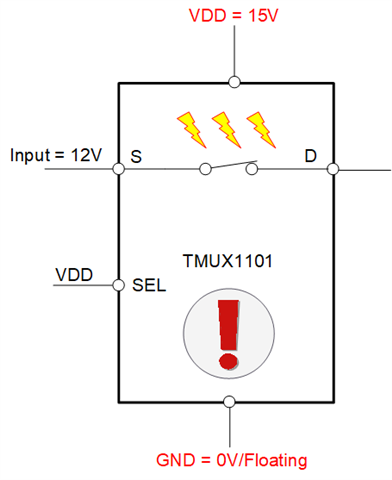
Moreover, the input voltages need to be disconnected as well to ensure an overvoltage event does not happen when the VDD is powered down.
The proper power down sequence should be the following:
- Disconnect the inputs
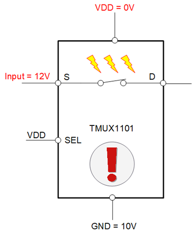
- Ramp both VDD/GND down at the same rate to ensure they are within an acceptable voltage range for the device. Removing one before the other completely can cause internal device damage.
Conversely, the power up sequence should be the following:
- Ramp both VDD/GND up at the same rate to ensure they are within an acceptable voltage range for the device. Applying one before the other completely can cause internal device damage.
- Connect inputs and ensure they are between the positive supply voltage and the GND voltage (Note: when ground shifting, the switch/multiplexer can only pass signals between the supply rail and GND shifted voltage, anything greater or less than these can cause damage to the device)