What is Fail-Safe Logic
Fail Safe Logic is a feature that allows voltages to be applied to the logic control pins before the supply pin, protecting the device and downstream devices from potential damage. This feature also allows for the logic inputs of the multiplexer to be interfaced with voltages greater than the supply pin as long as the voltages are below the absolute maximum rating.
How traditional multiplexers function
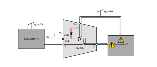
In a multiplexer without Fail-Safe Logic, the ESD diode prohibits any current flow from the logic pins to VDD under recommended operating conditions. When there is an instance where the VDD is exceeded past the maximum ratings in the datasheet, the signal on the select pin will only flow through the diode to the VDD rail. This typically happens at 0.5 V above VDD. Due to this, the device is protected from ESD events up to the datasheet's specification. When VDD = 0 V and the logic control pin has a voltage applied, a current can flow from the logic pin (labeled SEL in Figure 1 below) into the VDD rail. From there, it can back power subsystem B. This unwanted voltage can damage both the switch and subsystem B if their max ratings are violated. This is especially worrisome as the current might not be limited by the design.
Figure 1

How TI Fail-Safe Logic multiplexers function
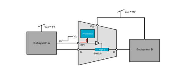
A TI multiplexer with Fail-Safe Logic will maintain a high impedance state on the signal path and digital logic pins when the supply is unpowered. This internal protection will prevent current from flowing into VDD and can be seen in Figure 2 below. The switch and subsystem B remain protected while there is voltage on SEL while VDD = 0 V. The Fail-Safe Logic feature also eliminates the need for a voltage translator if different voltages are used within the design. This is because the logic control pins can operate at higher voltage level than the supply pin voltage. For example, subsystem A, powered at 5 V, can control a multiplexer powered at 3.3 V. The signal levels still need to comply with the datasheet's ratings.
Figure 2

How can this affect your system?
Fail-Safe Logic minimizes system complexity by removing the need for power supply sequencing on the logic control pins. For example, the Fail-Safe Logic feature allows the logic control pins of the device to be ramped to 5.5 V while VDD = 0 V. Fail-safe logic also allows for maximum flexibility in system design by giving devices the ability to interface with a voltage greater than VDD on the logic control pins during normal operation. For example, the Fail-Safe Logic feature enables multiplexers to operate with VDD = 3.3 V while allowing the control pins to interface with a logic level of another device up to 5.5 V. Fail Safe logic can be found in all “TMUX” devices.
For more information on this topic, please watch this TI Precision Labs video

