This thread has been locked.

If you have a related question, please click the "Ask a related question" button in the top right corner. The newly created question will be automatically linked to this question.

SN74LVC2G66-Q1: Vi/o limits. Negative voltages OK?

Part Number: SN74LVC2G66-Q1
Other Parts Discussed in Thread: SN74LVC1G3157, SN74LVC2G66, TMUX1248, TMUX1119, OPA1678

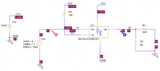
Hi - I have simulated the reference design for the LVC2G266 in PSPICE, the only change to the schematic being to tie the control pin permanently high.

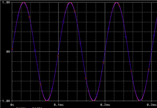
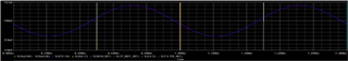
The image below is the resulting waveform seen either side of the switch - the result shows the output directly on top of the input which is as expected from a closed switch.

The datasheet gives the recommended voltage range for the I/O pins (Vi/o) as 0V to VCC. The simulation shows the device operating happily with an input of +1 V to -1V. Is the simulation correct? Would the negative voltages cause damage? Or am I misinterpretting the datasheet? 

The device I actually want to use is the 74LVC1G157 which has similar datasheet characteristics, but doesn't seem to have a PSpice model. I want to use the part as a switch for an analogue signal that will be biased around 0V (as per the simulation), but will be limited to very low signal amplitudes (less than +1mV to -1mV swing). Is this simulation also applicable to the 74LVC1G157?

  • The model is wrong. The ESD protection diodes would clamp signals that go 0.5 V beyond the power rails. This also applies to other analog switches like the SN74LVC1G3157.

    Below 0 V, correct operation is not guaranteed. (But it would probably work.)

    The 74LVC1G157 is not made by TI.

  • Hey Andrew, 

    I took a quick look and it would appear that the ESD diodes aren't actually modeled here. Not a huge surprise as the device is older and this model was released over 10years ago so there are little details that the model doesn't have. In real life applications, the ESD diode would clamp that voltage.

    I don't see a problem though in using the SN74LVC2G66 model to get an idea of the SN74LVC1G3157 behavior. 
    We also have a drop-in upgrade of the 3157 in the TMUX1248.

    Thanks,
    Rami

  • Thanks for the replies.

    My mistake, I had meant the 74LVC1G3157.

    The SN74LVC1G3157 datasheet gives a Vi/o range of -0.5V to VCC - would this safely (and cleanly) pass very low voltages biased around 0V. Presumably the -0.5V is taking into account the non-ideal nature of the protection diodes? 

  • The absolute maximum ratings guarantee that the device will not get damaged, and nothing more.
    The recommended operating conditions guarantee that the device will work correctly, with the electrical characteristics.

    At about 0.5 V, the protection diodes begin to conduct. 0.001 V is probably OK, but there is no guarantee.

  • Hey Andrew,

    As Clemens mentioned, you'd probably be fine with the 1mV swing but we can't guarantee any performance outside of the recommended conditions.

    Additionally, since you're working a low voltage swing you may benefit from looking into a precision muxltiplexer like the TMUX1119. The On resistance will be reduce with low leakage and charge injection 

    Thanks,
    Rami

  • Thanks again for all the reponses. I should have noticed that I had been looking at the maximum ratings when I saw the -0.5 limit.

    I have now simulated the analogue switch in the full circuit. The addition of the 74LVC2G66 massively slowed down the simulation to the extent that I had to leave it to run over the weekend, but it did complete.

    The following is the relevant part of the simulation with the resulting waveforms beneath.

    The final waveform image is of the input to the analogue switch zoomed right in. This seems to show that this signal has become biased around ~0.5mV. This figure closely aligns with the figure of 489.8uV which PSpice has annotated onto the schematic at this point. 

    Is this bias voltage created by the following opamp? I notice that the annotoation for the negative feedback for the preceding opamp also shows biasing at aorund 0.5mV. 

    I note the suggested alternative TMUX parts, I'm not sure they offer a significant advantage for me to justify the higher pricing. I am switching an audio signal in my application

  • Hey Andrew,

    I'm not an expert at op amps so the most I can really tell you here is that the mux itself shouldn't be the source of the bias. You could try to simulate the individual components and see where the bias occurs.
    The mux itself just behaves as a passive RC, so it's just passing through the signal that it sees. So in theory, if you're seeing 0V before the RC made with R45 and C29 and 500mV after, along with a 47uF cap on the opamp output then yes the 500uV would have to be sourced from the op amp and back through the mux. 

    I've looped in the team that supports the OP1678 to help better confirm that the 500uV output makes sense here. 

    Thanks,
    Rami

  • Hello Andrew,

    Yes, the 500uV offset voltage is coming from the OPA1678. The typical Vos is 500uV and can go up to +/-2mV at room temperature. Let me know if I can be of further assistance on your design. 

    Best Regards,

    Chris Featherstone