This thread has been locked.

If you have a related question, please click the "Ask a related question" button in the top right corner. The newly created question will be automatically linked to this question.

SN74CB3Q3253: Current ability and misdirection

Part Number: SN74CB3Q3253
Other Parts Discussed in Thread: UCC27211

Hi experts,

Our customer Ericsson is trying to use SN74CB3Q3253 in their power modules.

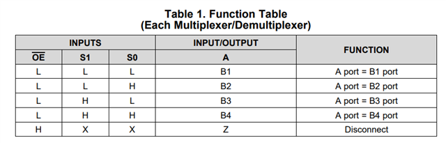
SN74CB3Q3253 to select different drive operation. To control different switch turn on and different voltage output.

The A side is linked to 3.3 V and the B side is linked to the input(HI,LI) of the UCC27211(Driver).

The customer has two concerns:

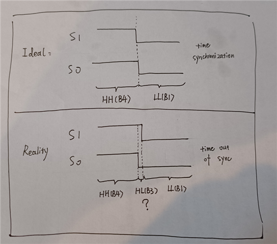
1)Will there be a transient misdirection ? For example, a short HL(B3) state occurs during the HH(B4) switch to LL(B1) due to timing synchronization. Will it lead to misdirection? 

2)Is the output current sufficient to drive the UCC27211 chip? (They are all signal chips, which should not be a problem, but the customer also wants to confirm because there is no maximum output current information in the datasheet.)

Thank you!

Best regards,

Tommy Mao 毛晓东

Field Application Engineer Intern| TI Semi Beijing Branch

  • Hello Tommy,

    1. If im understanding correctly when your mux is briefly in the B3 state it will connect  A port to B3 port and briefly have that as an on  signal path. This should not cause a transient misdirection but instead just show up as a slight delay when transitioning from B4 port being connected to A  to B1 being connected to A. 

    2.Also this device is a passive mux and does not redrive signals. It only passes them from A to B. So the current/voltage being passed coming from  A to B needs to be high enough to drive the UCC27211.  In addition this is the max current this device can handle on the inputs. 

    Please let me know if you have any further questions!

    Regards

    Kameron

  • Hi Kameron,

    Thank you for your reply. Yes, your understanding is correct. I would like to ask you a little bit more about question 1 .

    When S1 S0 falling edge is out of sync, S1=H,S0=L appears for a period of time, as shown in the figure below.

    Does this cause a short link between A and B3? Or will this state be cleared? Customers worry about that the B3 will misdirection.

    Thank you!

    Best regards,

    Tommy Mao

  • Hello Tommy,

    Yes this will cause a short link between A and B3. However to alleviate your customers concern about this, I would like to ask if the b3 output  is connected to another device?

    If not your customer could tie this B3 pin to ground and prevent the "misdirection" from affecting anything in your circuit!

    https://e2e.ti.com/support/switches-multiplexers-group/switches-multiplexers/f/switches-multiplexers-forum/1095179/faq-what-to-do-with-unused-pins-exposed-thermal-pads

    Please let me know what you think!

    Regards,

    Kameron

  • Hi Kameron

    B3 output is connected to another device.

    Can we avoid this misdirection by turning off the enable, s0s1 toggle, and turn on the enable? 

    Thank you!

    Best regards,

    Tommy Mao

  • Hi tommy,

    I think this should be fine and should get rid of the misdirection.

    So with this idea you should only toggle the s1 and s0 pins after resetting  or changing the enable pin from high to low. Never change the select pins while enable is low

    This should  eliminate any chance of a connection between a and b3

    Please let me know if there are anymore concerns!

    Regards