Other Parts Discussed in Thread: TMUX1208, CD74HCT4051, TMUX4051
Dear Technical Support, I have questions regarding P. 8 of CD74HC4051 device, Attached is the related datasheet & P. 8 of the related datasheet of this device for your easy reference..
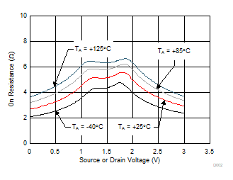
It seems that the circled area in P. 8 of CD74HC4051 datasheet shows 2 sets of Ron ( on resistance ) data, not sure what different test conditions in the test which will cause these 2 different sets of resistance values to happen?
Also, Io=1mA is shown in the "PARAMETERS" section for this set of test data, not sure if Io is changed to 10mA in the test, will the related ON resistance values be changed or remain the same as Io=1mA test case or not? If the resistance values do change when Io=10mA in the test, Not sure why the resistance value will change and will the resistance values be increased or decreased when Io=10mA?
Thanks and look forward to hearing from you when convenient.
yenwu lo
Acrobat Document_CD74HC4051.pdfAcrobat Document_CD74HC4051.pdf