This thread has been locked.

If you have a related question, please click the "Ask a related question" button in the top right corner. The newly created question will be automatically linked to this question.

SN74LVC1G3157: SN74LVC1G3157

Part Number: SN74LVC1G3157
Other Parts Discussed in Thread: OPA695

Tool/software:

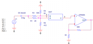
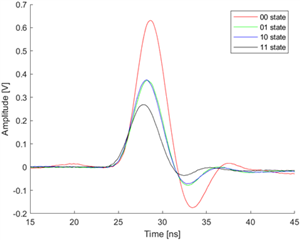
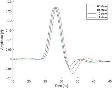
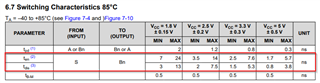
I design digital attenuator using SPDT. But this makes a signal delay by path. The graph below illustrates this delay. Both graph is OPA695 output signal. On the left, the signal is plotted as is, while on the right, the signal amplitude is normalized to the same level.

I need to understand why these delays occur. So I want to simulate the switch, but TI provides the IBIS model.

Can you explain how to model a switch using MOSFETs or BJTs?

  • Hello Shin,

    Our devices can be simulated using a discrete solution following this FAQ

    We also have an HSPICE model for the device you can simulate. 

    Regarding the delay concern, what is it exactly? What are you trying to accomplish? What do the different states represent? 

    Signal delay can be affected by many variables such as loading conditions and Ron.

    Toggling between the switches can also cause some delay. 

    Thanks,

    Nir 

  • I am designing an automatic gain control (AGC) system. To be precise, instead of changing the amplifier gain, I adjust the signal levels using a voltage divider.

    However, when I change the switch path (attenuation ratio), a delay occurs, which is undesirable for me. In the figure above, each state represents a switch path. My AGC consists of two stages with the same structure, so the 00 state means the switches are connected as (A-C, A-C), and the 11 state means they are connected as (B-C, B-C).

    I need to understand what is causing the delay and find a way to eliminate it.

  • Hello Shin,

    Understood thank you for elaborating. 

    The delay seems to be from the mux, since you mentioned when you switch the path the delay occurs. This is a natural behavior of the mux. 

    What voltage is the mux operating at? That delay can be up to 24ns, please see table below.

    What timing specs are you looking for? How much delay is too much? I might be able to recommend a better device to suit your application. 

    Thanks,

    Nir 

  • I operate the switch under a 5V supply condition. The delay difference between each state is 400 ps. Currently, I change the switch path manually using an MCU. To put it another way, the switch path does not change while the circuit is operational. So, I think switching characteristic don't cause the delay.

    Regardless of the current switch path, a constant ratio of voltage is always present between node B and node A.(A node = 10*B node) I am questioning whether this has any impact.

    My system is a lidar readout circuit, so delays above 100ps have a critical effect on performance.

  • Hello Shin,

    The voltage ratio between the nodes is x10 because of the voltage divider circuits. You can swap the values of R3 and R4 and see if it affects the delay.

    Thanks,

    Nir 

  • I checked effect of resistors and it obviously affects the delays. The delay difference decreases as R3 and R4 get larger.

    So, I suspect that the charge amount of the switch input increases the delay difference. Because my pulse has a 1.4ns rise time and a 1.6ns fall time, large R3 and R4 limit the signal amplitude (by RC constants).

    So, I want a simulation model of the switch to verify this hypothesis.

  • Hello Shin

    Understood, as I mentioned earlier these are the simulations we have for this device. 

    Since we don't have a PSpice model for it you can also simulate using a passive model, by following this FAQ

    Thanks,

    Nir