


Tool/software:
Most multiplexers use GPIO signals to switch between input and output connections. Another method of controlling a multiplexer is by using SPI. In place of GPIO control pins, a device controlled with SPI will have four pins: SDI, SDO, CS, and SCLK. Since it takes up to 4 pins to control a SPI device it’s more common to see it implemented on multiplexers with 8 or more channels. The mux has an internal SPI interface (as shown in figure 1) allowing for independently controlling the switches, resulting in a smaller footprint design.
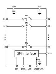
Figure 1 – SPI controlled multiplexer diagram
Address Mode
The TMUXS7614D is TI’s first true SPI controlled mux. It is a 1:1, single-pole, single-throw (SPST) 8-channel SPI controlled multiplexer. The SPI signal communication is defaulted to address mode, where the registers of the mux are accessed by a 16-bit SPI command bounded by the chip select line (/CS). With CRC enabled, the SPI signal will be a 24-bit command instead. Other than address mode the device can operate in burst and daisy chain modes. The SPI interface pins are SDI, SDO, SCLK, and /CS. During a SPI command, /CS has to be held low, while the data on the SDI line is captured by the device on the rising edge of SCLK. The data is sent out on the SDO line on the falling edge of SCLK. The SPI signal lanes are shown in Figure 2 below.
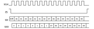
Figure 2 – SPI Address Mode Diagram
The first bit on the SDI line indicates whenever it is a read, or write command. If the bit is 1 it is a read, if it is 0 then it’s a write. The next seven bits are correlated to the target register address. The remaining eight bits are the data bits. They contain the data being sent on the SPI interface during a write command. In a read command the last eight bits on the SDI line are ignored, because during clock cycles 9 to 16, the SDO line sends out the data contained in the target address register. The data stored in the target register is sent out in the last eight bits on the SDO line on the falling edge of SCLK during a read command.
Burst Mode
Burst mode is enabled through the burst enable register. It allows the SPI to accept consecutive commands without the need to deassert the /CS line. It uses the same 16-bit command structure as the address mode to communicate with the device. The SDO line also operates similarly as in address mode.
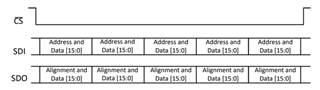
Figure 3 – SPI Burst Mode Diagram
Daisy Chain Mode
The TMUXS7614D can enter daisy chain mode by sending a 16-bit SPI command of 0x2500. Daisy chain mode allows to connect several devices in a daisy chain configuration. While in daisy chain mode, users have the capability to turn on or off individual switches on each device on the chain. All devices share the same /CS, SCLK, and VL lines. Each SDO line is connected to the SDI line of the next device on the chain, except the SDO line of the last device which is connected back to the MCU. In order to exit daisy chain mode a hardware reset is required. SPI signals in daisy chain are shown below in Figure 4. Table 1 shows the advantage of using a high channel mux controlled via SPI over GPIO.
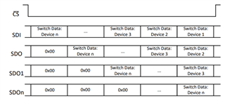
Figure 4 – SPI Daisy Chain Mode Diagram

Table 1 – GPIO vs SPI I/Os count comparison
For more information about the TMUXS7614D: