A related question is a question created from another question. When the related question is created, it will be automatically linked to the original question.
CD4066BM96 PIN9 output signal is abnormal. After replacing the previous batch of chips, the signal has returned to normal. Please help analyze the cause.
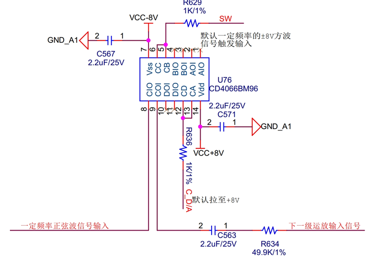
2. The following is the CD4066 input waveform and schematic diagram.
If I am understanding this properly, the "bad batch" was removed and replaced with a previous batch; Meaning no alterations, just a drop in replacement and the device worked properly?
Yes, replacing this batch of products with the previous batch of products will solve the problem without changing any hardware. The output waveform of PIN9 is as follows:
I am currently looking into the LOT information on the two batches. In regards to the pictures for pin9 output, you are saying the image on the right is the expected output and the image on the left is the abnormal one?
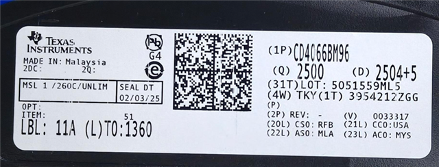
Do you happen to have the package with the LOT information, I have tried to find information on the devices from the picture but was not able to find the batch information?
Because you are saying this issue is just a batch error, since a previous batch does not have this issue.
In this case, you should be able to submit this to your local field contact and they can initiate the investigation with our group and we can conduct testing.
Is there any PCN between these two batches? Since this issue happened to all the new-batch devices. And for the customers, they have 25195pcs new version that they couldn't use. Could you help check their schematic again to confirm if this issue could be solved by changing components?
1. Is it possible to tie down all the floating I/O pins to prevent potential noise or unwanted behavior?
2. What is the intended function of these control pins with floating I/O connections? Are they being connected to VSS (-8V) elsewhere in the circuit?
3. How are these devices interfacing with the main board? I've noticed Pin 9 appears to simply output the input wave from Pin 8, which suggests the logic might be held high permanently rather than receiving the expected square wave input.