


Hi,
Could you please give us your advice as below ?
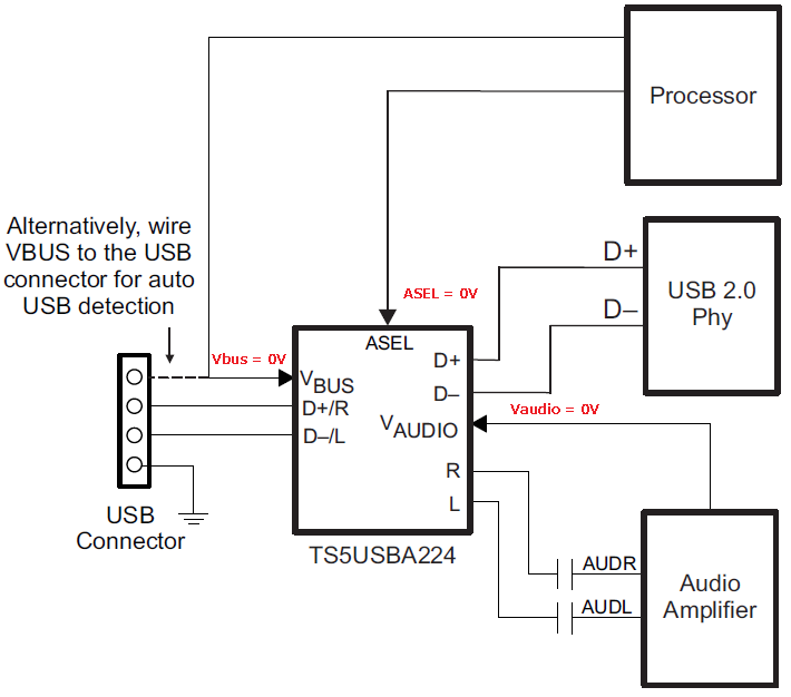
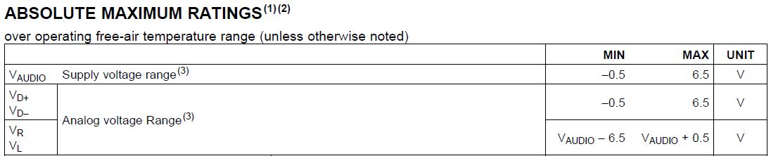
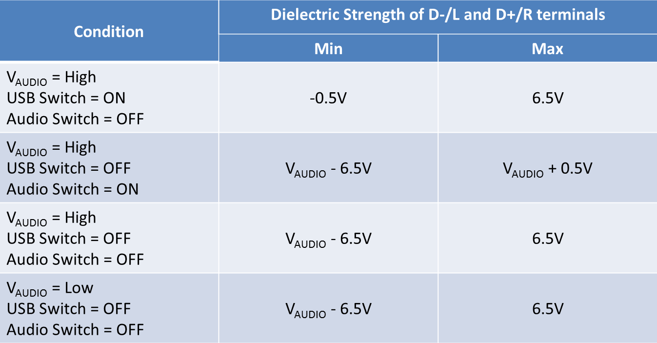
Q1. Absolute Maximum Ratings for D+/R and D-/L
Would you tell us the absolute maximum ratings for D+/R and D-/L as below ?
Which is correct although "-0.5V to 6.5V" and "Vaudio - 6.5V to Vaudio + 0.5V" are mentioned in the data sheet ?


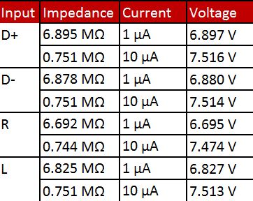
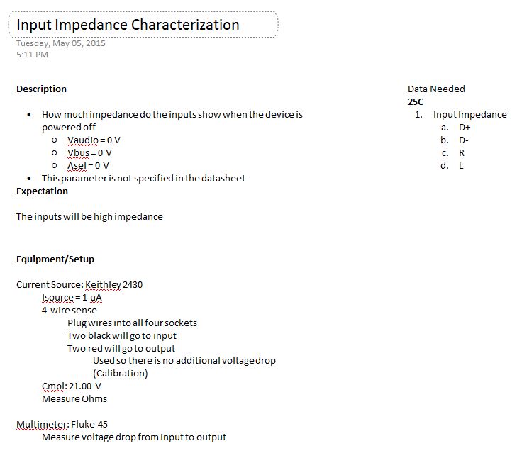
Q2. Input Impedance in the Power-off
Would you tell us the input impedance of D+/R, D-/L, D+, D-, R and L in the power-off ?
Is our understanding correct although we believe that it is Hi-Z ?
Q3. Input Signal Clipping in the power-off
Would you tell us whether the input signals(4Vpp@grounded center) are clipped by the esd protection diodes if they are input to D+/R, D-/L, R and L in the power-off ?
Moreover, would you tell us the clipped voltage if clipping ?
Best regards,
Kato


