This thread has been locked.

If you have a related question, please click the "Ask a related question" button in the top right corner. The newly created question will be automatically linked to this question.

CD4052B: Questions on Analog voltage range and clipping behaviour

Part Number: CD4052B
Other Parts Discussed in Thread: CD4053B, CD4051B

Hi, 

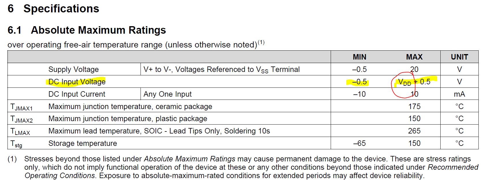
I am using CD4052B as analog mux for differential signals. Here are connection details.

VDD = 5V

VEE = -5V

VSS = GND

Please let me know if following understanding is correct.

  1. Analog input voltage range that can be passed through the mux is : -5V to +5V
  2.  If voltage at input pin(Channel pin) is 12V then output of the mux will be +5V, same way, if input is -12V then output of mux will be -5V. 
  3. There is no need for clipping diodes at analog-in pins, since there is inbuilt diode protecting the chip.

  • Yatin,

    You understanding is correct that the CD4052B as well as the CD4051B and CD4053B input signal range is limited to the supply voltage event if it isn't as obvious in the datasheet spec.  However we do not recommend exposing the device to voltages beyond the supply voltage range because it violates the absolute maximum ratings of the device and state in note (1) it increases the risk of permanently damaging or causing reliability issues. 

    You correctly stated there are protection diodes from the I/O path to the supply and ground and you can see they will begin to turn on about 0.5 V past the supply rails.  Because these are diodes the increase in voltage will exponentially increase the current through the device which could cause permeant damage or reliability concerns which is why the abs max table prevents this condition and limits the current to <10mA. 

    Thank you,

    Adam

  • Thanks a lot Adam for clearing it up !