This thread has been locked.

If you have a related question, please click the "Ask a related question" button in the top right corner. The newly created question will be automatically linked to this question.

CD74HC4051-Q1: question about how to use correctly

Part Number: CD74HC4051-Q1
Other Parts Discussed in Thread: CD74HCT4051-Q1

Hi Team

may I get your reply on the below ?

thanks.

[Q1] CD74HC4051-Q1 can bi-directional transfer analog signal in the range of ± 6V by VCC ~ VEE pins by setting VCC = +6V and VEE = ─6V.

         However, the control input signals for S0/S1/S2/E pins must be in the range of 0V ~ 6V by setting VCC = 6V and GND = 0V.

         Am I right ?


[Q2] If the bidirectional signal is within 0V ~ 5V range, we should provide VCC = 5V and VEE =  0V.

        In this case, can we connect GND pin and VEE pin directly together ?


[Q3] If the bidirectional signal is within ─2V ~ 5V range, we should provide VCC = 5V and VEE =  ─2V.

        In this case, GND pin will be 0V. under such situation, can we connect GND pin through capacitance to VEE pin ?

        If that how much cap value is OK ?

        Or we should not connect GND pin through any Cap to VEE ?

        Just I want to know our recommendation for this case.


[Q4] what it the Max possible Switching Frequency for S0/S1/S2 pins ?


[Q5] the transferable Min frequency(= -3dB) for A0~A7/COMOUT pins are 180 MHz at ± 4.5V for VCC ~ VEE ?


  • Hello Paul,

    I am assuming you are looking for an automotive qualified chip. Before are my answers.  Please feel free if you have further.

    [A1] You are right. If your input signals are within +/-6V, You have to set VCC = 6 and VEE = -6V. Control pins only refer to VCC and they have nothing to do with VEE. Please note, when VCC = 6V, VIH of control pins is 4.2V. In other words, VIH will vary with VCC. If you want a fixed VIH, please consider CD74HCT4051-Q1.

    [A2] When input signals are within 0~5V, VCC >= 5V and VEE <=0V. In other words, you can have VCC = 5V or VCC = 6V. You can short VEE to GND or connect VEE to -5V.

    [A3] VCC>=5V and VEE<=-2V. Decoupling capacitor between VEE and GND is recommended to be 1uF.

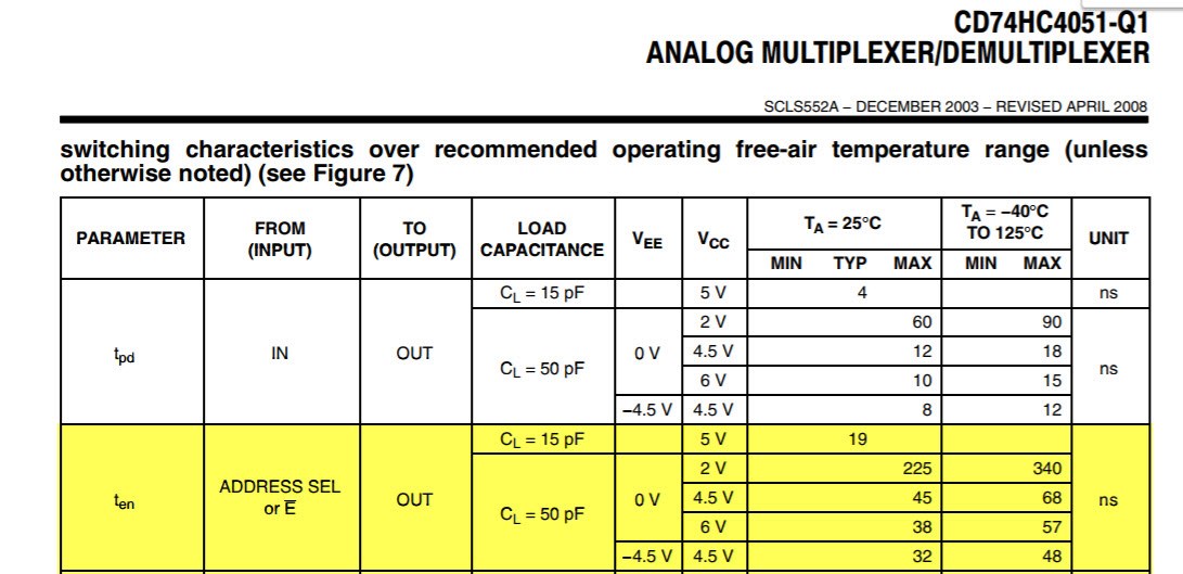
    [A4] Switching time is in nano-second range. Generally, for industrial and automotive designs, the switching time is not limiting. 

    [A5] Yes, you are right. Please be noted 180MHz bandwidth is only taken at 25C as the IC characteristic. You will expect slightly lower bandwidth when the temperature reaches 125C, though it does not decrease drastically. 

  • Hi Wang

    there are several Abs Max current in D/S.

    I can know the meaning for some, but also cannot catch themeaning for other some.

    Input Clamp Current will be the max current via internal ESD diode to VCC or GND if the control voltage of S0/S1/S2/E pins exceed VCC or GND pins.

    Output Clamp Current will be the max current via internal ESD diode to VCC or VEE if the transfered signal voltage of A0~A7/COMOUT pins exceed VCC or VEE pins.

    Switch Current will be the max allowable current that can be flowing via A0~A7 to COMOUT or Vice versa.

    what is the below things meaning ? may I get detail explanation to make me clearly understood ?

    [1] Continuous Current through VCC or GND = +- 50mA.

    [2] VEE current, IEE = - 20mA

  • Hi Paul,

    Continuous current flowing into or pulling out from VCC, GND (50mA) and VEE (20mA) means even if their voltage ratings are within datasheet, but board designers use a mechnism to force large current into these pins, these three pins can be permantly damaged.

    Fundamentaly, the current limiting requirement is calculated back from our internal metal trace width and transistor size. In normal operation, all these large current conditions are not expected to happen with our limited imagination.