This thread has been locked.

If you have a related question, please click the "Ask a related question" button in the top right corner. The newly created question will be automatically linked to this question.

SN74CBT3244: SN74CBT3244 output voltage issue

Part Number: SN74CBT3244
Other Parts Discussed in Thread: SN74CBTLV3245A, SN74CB3Q3244

Hi Experts:

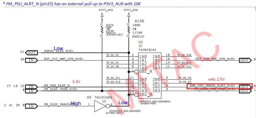
Customer use SN74CBT3244 as switch in PDB, enable signal is FM_SLED_PWRGD and circuit as below.

And they found the SMB_PSU_PMBUS_ALRT_N (pin5) of U2 only got 2.5V output but the source pin is 3.3V.

I removed all end device of SMB_PSU_PMBUS_ALRT_N<0>, and the voltage still 2.5V.


Do you know why the voltage will go lower than input side?  Do we need to add external pull-up on the output side?

But SN74CBT3244 should be a push pull output, i don't think we need pull up resistor at output, right?

Thanks.

  • Mark,

    The SN74CBT3244 device like all of the SN74CBTXXXX devices are passive single NFET switches and will clamp the output about a diode drop (~0.7V) from the supply voltage.  

    In the application note below you can see that the on-state resistance increases exponentially as the I/O signals approach the supply voltage.  The NFET gate is basically biased by the supply pin and as the I/O (source) voltage approaches the supply voltage it is reducing the gate to source voltage (Vgs) < the FET threshold voltage (Vt)  which turns off the FET.  

    If you would like to have a device that supports I/O voltage 0V to Vcc (rail to rail switch ) and not clamp the output you cannot use a single NFET type switch.  You can use either transmission gate architecture (NFET in parallel with PFET) like the SN74CBTLV3245A  or NFET with the gate biased with a charge pump like the SN74CB3Q3244.

    Thank you,

    Adam