This thread has been locked.

If you have a related question, please click the "Ask a related question" button in the top right corner. The newly created question will be automatically linked to this question.

CD4066B: how about the leakage current when bypass two channels of CD4066B

Part Number: CD4066B

Team,

We met two confusions from customer and need your advice here:

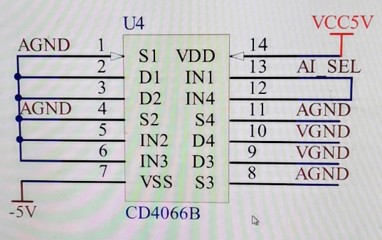
VDD=5V, VSS=-5V, 1~6 pin all connected to AGND, control AI_SEL signal to control CD4066B switch AGND or VGND, AI_SEL signal is 5V/-5V.

1. How about the leakage current this application will produce? B/C channels are connected to AGND. 

2. If IN2 and IN3 will also need to be connected to -5V even if B/C channels are bypassed? If not necessary, will it affect the leakage current? From customer's test result, it seems if they connect IN2/3 to the AGND, it will produce much higher leakage current than connect to -5V.

Thanks.

  • Hi Lucas,

    as mentioned in the datasheet, the off leakage current should be 10pA per channel. What are you measuring?

    The hire leakage can have different origins like the voltage over the protection diodes or in the CMOS switches. Can you precise the measured leakage currents?

    Is it an issue if they have to connect IN2/3 to -5V?

    Best regards,

    Ambroise

  • Hi Ambroise,

    Connect IN2/3 to -5V will not be a big problem, but why it will bring such a big impact on the leakage if connect to AGND not -5V?

    Thanks. 

  • Hi Lucas, 

    this depends on the exact internal structure of the MUX. The MOSFET switches where designed to work for +-7.5V supply so the structure is differen to other Muxes with typical 0-5V Vcc. Depending on the voltages applied to the gate/body of the transistor different the transistor has more or less leakages to the gate.

    Best regards,

    Ambroise