This thread has been locked.

If you have a related question, please click the "Ask a related question" button in the top right corner. The newly created question will be automatically linked to this question.

TS3L301: Needed information on the control impedance and current per lane.

Part Number: TS3L301
Other Parts Discussed in Thread: TS5MP646

Hi Team,

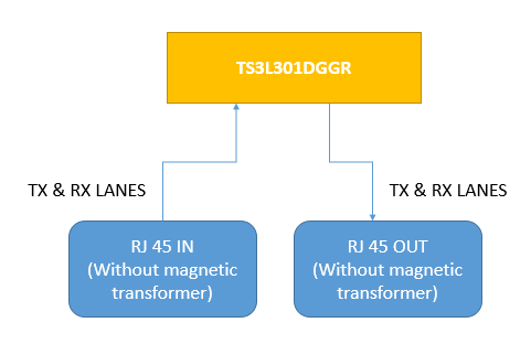
We are planning to use TS3L301DGGR part as analog switch in our project. We are just switching ON and OFF TX/RX lanes between RJ 45 IN and RJ 45 OUT using TS3L301DGGR as shown in below diagram. 

Could you please help us what will be issues if we do not maintain control impedance in the PCB for TX and RX lanes of RJ45 since we are going with two layer PCB? Please let me know whether there will be any loss of data in the signal lanes? We are not using magnetic transformer between RJ 45 and analog switch.

It would be very helpful if you also let me know what will be current flowing in each lane of RJ45 (1000B-T) without magnetic transformer. I found that the ON-state switch current of is TS3L301DGGR  +/- 128mA. Is TS3L301DGGR IC is advisable to use?

Regards,

Harshavardhan.K

  • Hello,

    Thanks for your question. Here are some layout guideline recommendations taken from a datasheet of another high-speed analog mux (TS5MP646), however PCB layout is a system design choice:

    • Place the supply de-coupling capacitors as close to the VDD and GND pin as possible. The spacing between the power traces, supply and ground, and the signal I/O lines, clock and data, should be a minimum of three times the race width of the signal I/O lines to maintain signal integrity.
    • The characteristic impedance of the trace(s) must match that of the receiver and transmitter to maintain signal integrity. Route the high-speed traces using a minimum amount of vias and corners. This will reduce the amount of impedance changes.
    • When it becomes necessary to make the traces turn 90°, use two 45° turns or an arc instead of making a single 90° turn.
    • Do not route high-speed traces near crystals, oscillators, external clock signals, switching regulators, mounting holes or magnetic devices.
    • Avoid stubs on the signal lines.
    • All I/O signal traces should be routed over a continuous ground plane with no interruptions. The minimum width from the edge of the trace to any break in the ground plane must be 3 times the trace width. When routing on PCB inner signal layers, the high speed traces should be between two ground planes and maintain characteristic impedance.
    • High speed signal traces must be length matched as much as possible to minimize skew between data and clock lines.

    The current driving the signal through the switch is dependent on the system. It is advisable to ensure the continuous current through the switch is within recommended operation conditions.

    Best regards,
    Kate