


Dear Team,
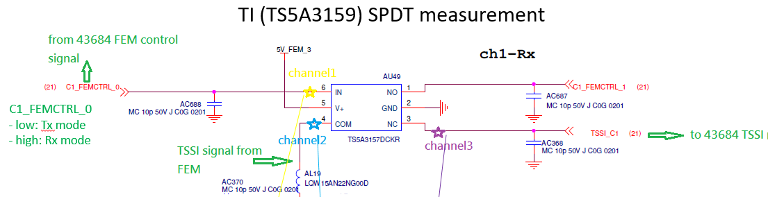
1.Is it necessary the NC and NO output pin have 50ohm during layout?
2.When Ch1(pin:6 IN) high, CH2 (pin:4 COM low), the CH3(pin:3 NC) didn't go low.
Is it because CH1 high just mean disconnect the COM to NC?
If I want to NC pin go low need to have pull low resistor? Or how to deal with it?
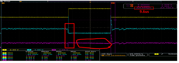
3. The COM pin have 22NH series inductance(AL19)
When input RF bandwidth 40MHz it will have rising time 9.6us
When input RD bandwidth 20MHz it will have rising time 24.8us, which causes the signal issue.
Any ideas can solve the rising time?

BR
Kevin


